Basic Photovoltaic Principles and Methods
Notice
This publication was prepared under a contract to the United States Government. Neither the United States nor the United States Department of Energy, nor any of their employees, nor any of their contractors, subcontractors, or their employees, makes any warranty, expressed or implied, or assumes any legal liability or responsibility for the accuracy, completeness or usefulness of any information, apparatus, product or process disclosed, or represents that its use would not infringe privately owned rights.
Printed in the United States of America
Available in print from:
Superintendent of Documents
U.S. Government Printing Office
Washington, DC 20402
Available in microfiche from:
National Technical Information Service
U.S. Department of Commerce
5285 Port Royal Road
Springfield, VA 22161
Stock Number: SERIISP-290-1448
Information in this publication is current as of September 1981
This book presents a nonmathematical explanation of the theory and design of PV solar cells and systems. It is written to address several audiences: engineers and scientists who desire an introduction to the field of photovoltaics, students interested in PV science and technology, and end users who require a greater understanding of theory to supplement their applications.
The book is effectively sectioned into two main blocks: Chapters 2-5 cover the basic elements of photovoltaics-the individual electricity-producing cell. The reader is told why PV cells work, and how they are made. There is also a chapter on advanced types of silicon cells. Chapters 6-8 cover the designs of systems constructed from individual cells-including possible constructions for putting cells together and the equipment needed for a practioal producer of electrical energy. In addition, Chapter 9 deals with PV's future. Chapter 1 is a general introduction to the field.
The authors of this document are Paul Hersch and Kenneth Zweibel. They would like to thank their colleagues at the Solar Energy Research Institute's Solar Electric Conversion Division who reviewed the manuscript for technical accuracy: Richard Bird, Kathryn Chewey, Satyen Deb, Keith Emery, Kay Firor, Steve Hogan, Larry Kazmerski, Jack Stone, Thomas Surek, and Simon Tsuo. Gary Cook and Richard Piekarski of the Technical Information Office, who designed the document, were also helpful readers. Graphic Directions of Boulder, Colorado, was responsible for the text's figures, often with valuable improvements. Ray David was the cover artist. Vincent Rice of the Photovoltaics Program Office at DOE was supportive throughout, giving impetus to the project.
Chapter 1
Introduction
Photovoltaic systems behave in an extraordinary and useful way: They react to light by transforming part of it into electricity. Moreover this conversion is novel and unique, since photovoltaics:
| • | Have no moving parts (in the classical mechanical sense) to wear out |
| • | Contain no fluids or gases (except in hybrid systems) that can leak out, as do some solar-thermal systems |
| • | Consume no fuel to operate |
| • | Have a rapid response, achieving full output instantly |
| • | Can operate at moderate temperatures |
| • | Produce no pollution while producing electricity (although waste products from their manufacture, and toxic gases in the event of catastrophic failure and disposal may be a concern) |
| • | Require little maintenance if properly manufactured and installed |
| • | Can be made from silicon, the second most abundant element in the earth's crust |
| • | Are modular permitting a wide range of solar-electric applications such as
|
| • | Have a relatively high conversion efficiency giving the highest overall conversion efficiency from sunlight to electricity yet measured |
| • | Have wide power-handling capabilities, from microwatts to megawatts |
| • | Have a high power-to-weight ratio making them suitable for roof application |
| • | Are amenable to on-site installation, i.e., decentralized or dispersed power |
Clearly, photovoltaics have an appealing range of characteristics.
However, there are ambivalent views about solar, or photovoltaic, cells' ability to supply a significant amount of energy relative to global needs.
| • | Those pro, contend: Solar energy is abundant, inexhaustible, clean, and cheap. |
| • | Those can, claim: Solar energy is tenuous, undependable, and expensive beyond practicality. |
There is some truth to both of these views. The sun's energy, for all practical purposes, is certainly inexhaustible. However, even though sunlight striking the earth is abundant, it comes in rather a dilute form.
THE SUN
The sun is an average star. It has been burning for more than 4-billion years, and it will burn at least that long into the future before erupting into a giant red star, engulfing the earth in the process.
Some stars are enormous sources of X-rays; others mostly generate radio signals. The sun, while producing these and other energies, releases 95% of its output energy as light, some of which cannot be seen by the human eye. The peak of its radiation is in the green portion of the visible spectrum. Most plants and the human eye function best in green light since they have adapted to the nature of the sunlight reaching them.
The sun is responsible for nearly all of the energy available on earth. The exceptions are attributable to moontides, radioactive material, and the earth's residual internal heat. Everything else is a converted form of the sun's energy: Hydropower is made possible by evaporation-transpiration due to solar radiant heat; the winds are caused by the sun's uneven heating of the earth's atmosphere; fossil fuels are remnants of organic life previously nourished by the sun; and photovoltaic electricity is produced directly from sunlight by converting the energy in sunlight into free charged particles within certain kinds of materials.
The Nature of Light Energy
Light is energy. You need only touch a black surface exposed to the sun to realize this fact. An understanding of the nature of light will help in comprehending how solar cells work.
The sun's light looks white because it is made up of many different colors that, combined, produce a white light. Each of the visible and invisible radiations of the sun's spectrum has a different energy. Within the visible part of the spectrum (red to violet), red is at the low-energy end and violet is at the high-energy endhaving half again more energy as red light. Light in the infrared region (which we can't see but feel as heat) has less energy than that in the visible region. Light in the ultraviolet region(which is invisible but causes the skin to tan) has more than that in the the visible region.
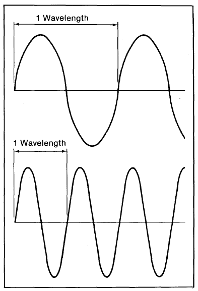
Visible light represents only a tiny portion of a vast radiation spectrum. Studies of light and similar radiation show that the way in which one light ray interacts with another or other physical objects often can be explained as if light were moving as a wave. For this reason it is useful to characterize light radiation by parameters associated with waves. All waves have a certain distance between peaks (called the wavelength) (Figure 1-1). This wavelength can also be expressed as a frequency (the number of peaks in a specified distance or during a specified time of propagation). Thus a wave with a long distance between peaks (long wavelength) has a lower frequency than one with a shorter wavelength (many peaks). (Note that frequency and wavelength vary inversely.) For light waves, the energy associated with the wave increases as the frequency increases (wavelength decreases). Red light has a wavelength of about 0.66 micrometers* (453 terahertz, or about 3 x 10 - 12 ergs [3 x 10 - 24 kW-h per "particle" of light [photon]), violet light, about 0.44 (682 terahertz, or about 4.5 x 10 -12 ergs [4.5 x 10 - 24 kW-h] per photon). X-rays are even shorter and more energetic. Microwaves (of the order of centimeters in wavelength) are longer than light waves and carry less energy.
Figure 1-1. Light interacts with itself and objects in a way that suggests it is a wave. Two ideal waves are depicted in the illustration. The top wave has a wavelength (the distance between two points where its shape repeats) that is twice that for the bottom one.
Every wave also has a frequency of propagation that is inversely related to the wavelength in a manner depending on the velocity of propagation of the wave: specifically, wavelength equals velocity of propagation divided by frequency. In the illustration the bottom wave has half the wavelength but twice the frequency of the one above it.
Sunlight Reaching Earth
Even though the sun ranks as a run-of-the-mill star, it releases a huge quantity of energy in terms of human capacity or need. Power output per second is 3.86 × 10²⁰ megawatts (MW), several billion times the electric capacity of U.S. utilities. This energy fills the solar system, bathing the earth's atmosphere with a near constant supply of 1.37 kilowatts per square meter (kW/m2) .
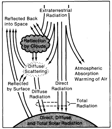
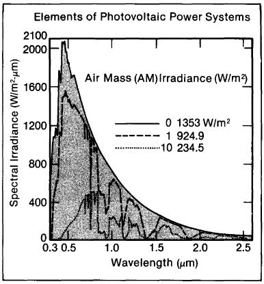
Not all of the direct sunlight incident on earth's atmosphere arrives at the earth's surface (Figure 1-2). The atmosphere attenuates many parts of the spectrum (Figure 1-3). For example, X-rays are almost totally absorbed before reaching the ground. A good percentage of ultraviolet radiation is also filtered out by the atmosphere. Some radiation is reflected back into space. Some is randomly scattered by the atmosphere, which makes the sky look blue.
It is valuable to relate the amount of sunlight at the earth's surface to the quantity, or air mass (AM), of atmosphere through which the light must pass. Radiation arriving at the surface of the earth is measured against that reaching the fringes of the atmosphere, where there is no air, and the air mass is zero (AMO). The light of the high-noon sun (and under further specified conditions) passes through an air mass of one (AM1). The intensity of the sunlight reaching the ground weakens for sun angles approaching the horizon since the rays have more atmosphere, or air mass, to penetrate. The atmosphere is a powerful absorber and can cut the sun's energy reaching the earth by 50% and more.
The peak intensity of sunlight at the surface of the earth is about 1 kW/m2. However, not all areas of the earth get the same average amounts of sunshine throughout the year. The most intensely bathed areas lie between 30o north and 30o south latitude, since these areas have the least cloud cover. There also are, of course, seasonal radiation variations caused by the tilt of the earth with respect to the sun. Thus, the winter sun will daily provide less than 20% of the summer sun's energy at some locations because it is lower in the sky and the days are shorter.
*A micrometer (J.lm) is one millionth of a meter.
Figure 1-2. The earth's atmosphere and clouds affect the way in which the sun's light reaches the surface of the earth.
All of these factors affecting the amount of local radiation on earth have to be taken into account when designing photovoltaic systems. The sun may be a constant source of energy, but at the earth's surface, the distribution of its energy and the constancy of its radiation are hardly ideal. A good PV system cannot be designed without providing for the variations associated with the energy spectrum and its local availability.
PHOTOVOLTAICS-A HISTORY
The physical phenomenon responsible for converting light to electricity-the photovoltaic effect-was first observed in 1839 by a French physicist, Edmund Becquerel. Becquerel noted a voltage appeared when one of two identical electrodes in a weak conducting solution was illuminated. The PV effect was first studied in solids, such as selenium, in the 1870s. In the 1880s, selenium photovoltaic cells were built that exhibited 1%-2% efficiency in converting light to electricity. Selenium converts light in the visible part of the sun's spectrum; for this reason, it was quickly adopted by the then-emerging field of photography for photometric (light-measuring) devices. Even today, light-sensitive cells on cameras for adjusting shutter speed to match illumination are made of selenium.
Figure 1-3. Light from the sun at the outer fringes of the earth's atmosphere (AMO) covers a broad range of wavelengths (frequencies). As the light comes through the earth's atmosphere it is selectively absorbed by certain elements in the atmosphere, resulting in chinks in the spectral distributions AM1 and AM10. Irradiance diminishes as the atmospheric mass (AM) numbers increase, since less light can penetrate the "thicker" atmospheres associated with the sun's not being directly overhead on a sparkling clear day (AM1). (Note that the frequency scale runs opposite to the wavelength scale.)
Selenium cells have never become practical as energy converters because their cost is too high relative to the tiny amount of power they produce (at 1% efficiency). Meanwhile, work on the physics of PV phenomena has expanded. In the 1920s and 1930s, quantum mechanics laid the theoretical foundation for our present understanding of PV. A major step forward in solar-cell technology came in the 1940s and early 1950s when a method (called the Czochralski method) was developed for producing highly pure crystalline silicon. In 1954, work at Bell Telephone Laboratories resulted in a silicon photovoltaic cell with a 4% efficiency. Bell Labs soon bettered this to a 6% and then 11% efficiency, heralding an entirely new era of power-producing cells.

Figure 1-4. In the future every home may supply at least part of its electric needs using root-mounted photovoltaics.
A few schemes were tried in the 1950s to use silicon PV cells commercially. Most were for cells in regions geographically isolated from electric utility lines. But an unexpected boom in PV technology came from a different quarter. In 1958, the U.S. Vanguard space satellite used a small (less than one-watt) array of cells to power its radio. The cells worked so well that space scientists soon realized the PV could be an effective power source for many space missions. Technology development of the solar cell has been a part of the space program ever since.
Besides the space program, another source, the transistor industry, contributed greatly to solar-cell technology. Transistors and PV cells are made from similar materials, and their workings ate determined by many of the same physical mechanisms. An enormous amount of research and development has been expended in improving the ever-useful transistor, and there has been a constant spin-off of valuable information in relation to solar cells. The situation has reversed recently: Much of the research being done in PV is affecting transistor technology.
Today, photovoltaic systems are capable of transforming one kilowatt of solar energy falling on one square meter into about a hundred watts' of electricity. Onehundred watts can power most household appliances: a television, a stereo, an electric typewriter, or a lamp. In fact, standard solar cells covering the sun-facing roof space of a typical home can provide about 8500-kilowatthours of electricity annually, which is about the average household's yearly electric consumption. By comparison, a modern, 200-ton electric-arc steel furnace, demanding 50,000 kilowatts of electricity, would require about a square kilometer of land for a PV power supply.
Certain factors make capturing solar energy difficult. Besides the sun's low illuminating power per square meter, sunlight is intermittent, affected by time of day, climate, pollution, and season. Power sources based on photovoltaics require either back-up from other sources or storage for times when the sun is obscured.
In addition, the cost of a photovoltaic system is far from negligible (electricity from PV systems in 1980 cost about 20 times* that from conventional fossilfuel- powered systems).
Thus, solar energy for photovoltaic conversion into electricity is abundant, inexhaustible, and clean; yet, it also requires special techniques to gather enough of it effectively.
*This is a very subjective figure because economic factors such as interest rates, taxes, tax deductions, competitive costs, and inflation are inherently variable; twentyfold is meant only as an estimate.
BIBLIOGRAPHY
Bailey, Robert L. 1980. Solar Electrics Research and Development. Ann Arbor, MI: Ann Arbor Sciences; pp. 2-186.
Cheremisinoff, Paul N.; Dickinson, William C. (eds.). 1980. Solar Energy Technology Handbook, Part A. New York, NY: Marcel Dekker, Inc.; pp. 1-167.
Dixon, A.E.; Leslie, J.D. (eds.). 1979. Solar Energy Conversion. New York, NY: Pergamon Press; pp. 1-37.
Rauschenbach, H.S. 1980. Solar Cell Array Design Handbook. New York, NY: Van Nostrand Reinhold Co.; pp. 6-14, 155-160.
Chapter 2
The Photovoltaic (PV) Effect
HIGHLIGHTS
The photovoltaic (PV) effect is the basis of the conversion of light to electricity in photovoltaic, or solar, cells. Described simply, the PV effect is as follows: Light, which is pure energy, enters a PV cell and imparts enough energy to some electrons (negatively charged atomic particles) to free them. A built-in-potential barrier in the cell acts on these electrons to produce a voltage (the so-called photovoltage), which can be used to drive a current through a circuit.
This description does not broach the complexity of the physical processes involved. Although it is impossible here to cover fully all the phenomena that contribute to a PV-generated current, it is possible to go deeply enough into these phenomena to understand how an effective cell works and how its performance can be optimized. We can do this by answering some fundamental questions about processes central to the working of a PV cell:
- What does it mean to say that an electron is freed?
- Where is it freed from?
- Where does it go?
- What is the potential barrier that acts on the free electrons?
- How is it formed?
- What does it do?
- Once acted on by the potential barrier, how do the free charges produce a current?
We shall take the silicon cell as a model. Silicon is a widely used, typical cell material; understanding the silicon cell is a good groundwork for understanding any PV cell. We shall start by reviewing some of silicon's basic atomic characteristics.
AN ATOMIC DESCRIPTION OF SILICON
All matter is made from atoms. They, in turn, are composed of three kinds of particles: protons, neutrons, and electrons. Protons (positively charged) and electrons (negatively charged) attract each other; neutrons are not electrically attracted to either and are said to be neutral. The positively charged protons and the neutral neutrons reside in a nucleus, the close-packed center of the atom. The electrons-much lighter than the protons (or neutrons)-orbit the nucleus. Although an atom contains charged particles, overall it is electrically neutral because it has the same number of protons and electrons.
Different atoms have different numbers of protons. For every proton in an atom's nucleus, there is an electron orbiting the nucleus. The orbital locations (and the motion of the electrons about their own axis) are determined by the energy of the electrons. The electrons, in particular those furthest from the nucleus, interact with electrons from other atoms and determine the way in which like or dissimilar atoms combine into larger structures such as solids.
The silicon atom has fourteen electrons arranged in such a way that the outer four can be given to, accepted from, or shared with another atom. These four outer electrons are called valence electrons.
Large numbers of silicon atoms, through their valence electrons, can bond together to form a solid. As a solid, each silicon atom usually shares each of its four valence electrons with another silicon atom. Each basic silicon unit, forming a tetrahedral arrangement, thereby contains five atoms (the one silicon atom plus the four others it shares electrons with).
Each atom in the silicon solid is held in place at a fixed distance and angle with each of the atoms with which it shares a bond. This regular, fixed formation of a solid's atoms is called a crystal lattice.
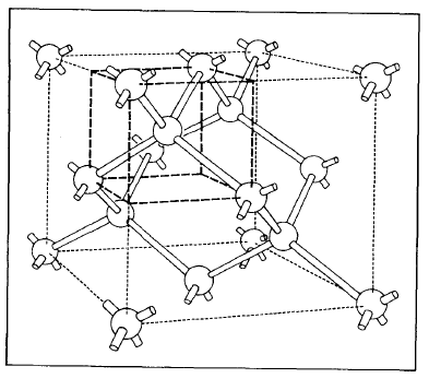
Solids can form from several differently shaped crystal lattices. (All solids are not crystalline, however; some can have multiple crystalline forms and/or none at all.) For silicon (Figure 2-1) the atoms are located so as to form the vertices of a cube with single atoms centered at each of the faces of the cubic pattern. The cubic arrangement repeats throughout the crystal.
THE EFFECT OF LIGHT ON SILICON
When light strikes a silicon crystal, it may be reflected, be absorbed, or may go right through. Let's concentrate on the light that is absorbed. Usually when light of relatively low energy is absorbed by a solid, it creates heat without altering the electrical properties of the material. That is, low-energy light striking a silicon crystal causes atoms of silicon to vibrate and twist in their bound positions, but do not break loose. Similarly, electrons in bonds also gain more energy and are said to attain a higher energy level. Since these energy levels are not stable, the electrons soon return to their original lower energy levels, giving off as heat the energy they had gained.
Figure 2-1. Representation of the silicon crystal lattice arrangement.
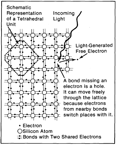
Light of greater energy can alter the electrical properties of the crystal. If such light strikes a bound electron, the electron is torn from its place in the crystal. This leaves behind a silicon bond missing an electron and frees an electron to move about in the crystal. A bond missing an electron, rather picturesquely, is called a hole. An electron free to move throughout the crystal is said to be in the crystal's conduction band (Figure 2-2), because free electrons are the means by which electricity flows. Both the conduction-band electrons and the holes play important parts in the electrical behavior of PV cells. Electrons and holes freed from their positions in the crystal in this manner are said to be light-generated electron-hole pairs.
A hole in a silicon crystal can, like a free electron, move about the crystal. The means by which the hole moves is as follows: An electron from a bond near a hole can easily jump into the hole, leaving behind an incomplete bond, i.e., a new hole. This happens fast and frequently-electrons from nearby bonds trade positions with holes, sending holes randomly and erratically throughout the solid. The higher the temperature of the material, the more agitated the electrons and holes and the more they move.
The generation of electrons and holes by light is the central process in the overall PV effect, but it does not itself produce a current. Were there no other mechanism involved in a solar cell, the light-generated electrons and holes would meander about the crystal randomly for a time and then lose their energy thermally as they returned to valence positions. To exploit the electrons and holes to produce an electric force and a current, another mechanism is needed-a built-in "potential" barrier. *
Figure 2-2. Light of sufficient energy can generate electron-hole pairs in silicon, both of which move for a time freely throughout the crystal.
8The barrier is called "potential" because it is an electrical phenomenon having to do with how much energy a particle (electron or hole) would "potentially" gain if that particle encountered the barrier and were accelerated.
THE POTENTIAL BARRIER
The Function of the Barrier
A PV cell contains a barrier that is set up by opposite electric charges facing one another on either side of a dividing line. This potential barrier selectively separates light-generated electrons and holes, sending more electrons to one side of the cell, and more holes to the other. Thus separated, the electrons and holes are less likely to rejoin each other and lose their electrical energy. This charge separation sets up a voltage difference between either end of the cell (Figure 2-3), which can be used to drive an electric current in an external circuit.
Figure 2-3. A potential barrier ina solar cell separates light-generated charge carriers, creating a voltage.
Forming the Barrier
There are several ways to form a potential barrier in a solar cell. One is to slightly alter the crystal so that its structure on either side of the dividing line is different.
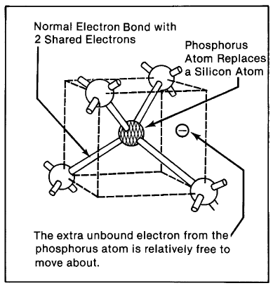
The Negative-Carrier (Donor) Dopant. As previously indicated, silicon has four valence electrons, all of which are normally part of bonds in a silicon crystal. Suppose by some means we introduce an impurity into an otherwise pure silicon crystal by substituting for a silicon atom an atom such as phosphorus, having five valence electrons. The impurity atom would occupy the same position in the crystal as a normal silicon atom, supplying an electron for each of silicon's four bonds. But because the phosphorus atom has one extra valence electron, there would be one electron with no bond to share (Figure 2-4). Compared with a bound electron, the impurity atom's extra electron is relatively free. In fact, at room temperature there is enough thermal energy in the crystal to shake this electron loose, despite the fact that it would leave behind a positively charged impurity atom.* This free electron from the impurity has no hole (empty bond) into which it may readily drop, and it behaves as if it were a permanent member of the crystal's conduction band, always ready to be part of an electric current.
*A charged atom is called an "ion."
A silicon crystal with numerous substituted phosphorus atoms would have many free, conductionband electrons and a similar number of positive impurity ions locked into the crystal's structure. Overall, the whole crystal would remain neutral, since there are just as many positive ions as free electrons; but the crystal's electrical properties would have been drastically altered.
Figure 2-4. When an impurity atom such as phosphorus with five valence electrons is substituted into a silicon crystal, it has an extra, unbonded electron.
Impurities introduced in this way are called dopants, and dopants that have one extra valence electron (such as phosphorus introduced into a. silicon crystal) are called donors because they donate an electron to the crystal. Such a donor-doped crystal is known as n-type because it has free negative charges.
Altering silicon by introducing a donor dopant is part of the process used to produce the internal potential barrier. But n-type silicon cannot of itself form the barrier; other, slightly altered silicon is also necessary, this kind with electrical properties opposite those of the n-type silicon.*
*There are other ways of forming the barrier such as contacting the silicon with metal or with charged silicon dioxide; these are described in later chapters.
The Positive-Carrier (Acceptor) Dopant. An appropriately altered material can be formed by substituting into the silicon crystal, impurity atoms with one fewer valence electron than silicon. An impurity atom with three valence electrons (such as boron) would sit in the position of the original silicon atom, but one of its bonds with the silicon would be missing an electron, i.e., there would be a hole (Figure 2-5). As we saw before, holes can move about almost as freely as conduction-band electrons. In this way, a silicon crystal doped with many such boron atoms has many holes that act as if they were free positive charges moving throughout the crystal lattice.
Figure 2-5. A three-valence-electron impurity (such as boron) in a silicon crystal is normally bonded, except one of the bonds is missing an electron, i.e., is a hole.
A three-valence-electron impurity in a silicon crystal is called an acceptor because its holes accept electrons (normally bonded valence electrons or conductionband electrons) from the rest of the silicon crystal. An acceptor-doped silicon material is called p-type because of the presence of free positive charges (the moving holes).
In a p-type material, positive charges are the so-called majority (charge) carriers because they far outnumber any free electrons that in p-type materials are referred to as minority carriers. In an n-type material, where the doping is reversed, electrons (negative charges) are the majority carriers and holes the minority carriers.
The Junction. A line dividing n-type from p-type silicon establishes the position of a potential barrier essential to the operation of a solar cell. To see how this barrier comes into being, let's take a look at the junction between the two materials (the area in the immediate proximity of the two surfaces). In the p-type material, there are excess holes; in the n-type material, excess electrons (Figure 2-6a). When the nand p materials are in contact, free electrons in the n-type material adjacent to the many holes in the p-type material at the junction will jump into the p-type material, filling the holes. Also, valence band electrons on the n-type side can jump into holes on the adjacent p-type side, which is equivalent to a hole moving over into the n-type material (for simplicity, this is not shown in Figure 2-6). This charge transference process happens rapidly along the dividing line (junction), sending huge numbers of electrons to 'the p-type side and holes to the n-type side (Figure 2-6b). This causes an immediate imbalance of charge: more negative charges (extra electrons) along the p-type side of the interface, more positive charges (ions) along the n-type side (Figure 2-6c).
When electrons move over into the p-type material during junction formation, they find holes in the silicon bonds and drop into them. In like manner, holes that transfer to the n-type side are quickly filled by the n-type side's numerous extra electrons. Consequently, carriers that form the junction lose their freedom of movement. Thus, although a charge imbalance exists at the junction, there are very few free electrons on the p-type silicon side to be pulled back to the n-type side, and very few free holes on the n-type side to be transferred back to the p-type material. So, the charge imbalance stays fixed in place.
The Barrier. The process of charges moving across the junction to create a charge imbalance in the abovedescribed manner does not continue indefinitely. Charged carriers that have already crossed the junction set up an electric force (field) that acts as a barrier opposing the further flow of free carriers. As more carriers cross the junction, the barrier enlarges, making it increasingly difficult for other carriers to cross. Eventually, an equilibrium is established where (statistically speaking) no more electrons or holes switch sides. This creates a fixed potential barrier at the junction (the barrier to which we have been referring since the beginning), with the n-type side adjacent to the junction being positively charged and the p-type side adjacent to the junction being negatively charged. The "height" (that is, the strength of the electric force) of the barrier, it should be noted, depends upon the amount of dopant in the silicon-the more the dopant, the more charge imbalance induced and the greater the barrier's ability to separate charges.
Let us note some qualities of the barrier (Figure 2-6d). It opposes the crossing of majority charge carriers. That is, electrons in the n-type material would have to climb the barrier against the built-in field to enter the p-type material. Similarly, holes in the p-type region are held back from entering the n-type region. Note also that minority carriers are not hindered by the barrier. In fact, free electrons on the p-type side- of which there are very few, being the minority carrier there-are driven by the junction field to the opposite, n-type side. The same is true of holes driven from the n-type side. But normally (under no illumination) there are so few minority carriers on their respective sides that their movement is nil; and what there is, is balanced by the few majority carriers that randomly assume enough energy to cross the barrier. This selective barrier at the junction is the means of separating charges during electron-hole generation under illumination. It is the key to the production of a PV electric current.

Figure 2-6. During junction formation, electrons move from the n-type silicon into the p-type, while holes move in the opposite direction. Movement of electrons into the p-type silicon and holes into the n-type silicon builds up a fixed potential barrier at the junction opposing the further movement of free carriers and creating a state of equilibrium.
The Potential Barrier in Action
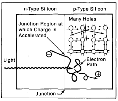
For illustrative purposes, suppose light striking the PV cell has enough energy to free an electron from a bond in the silicon crystal. This creates an electronhole pair-a free electron and a free hole. Suppose further that the electron-hole pair is generated on the p-type silicon side of the junction. An electron from such an electron-hole pair has only a relatively short time during which it is free because it is very likely to combine with one of the numerous holes on the p-type side. But solar cells are designed so that in all probability the electron will meander around the crystal and encounter the junction before it has the chance to combine with a hole (Figure 2-7). (Were it to combine with a hole, it would lose its energy as heat and be useless as far as PV electric current is concerned.)
Once the free electron is within the field of the junetion(which is limited to the junction's immediate vicinity), the electron is accelerated across the barrier (by the barrier's charge imbalance) into the n-type silicon. Since there are very few holes on the n-type side of the junction, the electron is no longer in great danger of recombining. Moreover, there is very little chance of its returning to the p-type side because it would have to buck the repulsion of the junction's field (climb the barrier), expending energy it usually doesn't have.
The hole partner of this electron-hole pair, however, remains on the p-type side of the junction because it is repelled by the barrier at the junction. It is not in danger of recombining because there are already a predominance of holes on the p-type side.
Figure 2-7. A photogenerated electron on the p-type side usually has enough time to bounce randomly around the crystal and encounter the junction before it can combine with a hole.
A similar situation occurs when the electron-hole pairs are generated by light on the n-type side of the junction. This time the freed electrons remain on the n-type side, being repelled by the barrier. Meanwhile, most of the holes encounter the junction before chancing to recombine. They cross the junction into the p-type side when normally bound electrons from the p-type side jump the junction and fill the holes. Once on the p-type side, the holes move around unhindered, and there are very few free electrons available to fill them.
Because illumination and charge separation causes the presence of uncombined excess negative charges on the n-type side and excess holes on the p-type side, a charge imbalance exists in the cell.
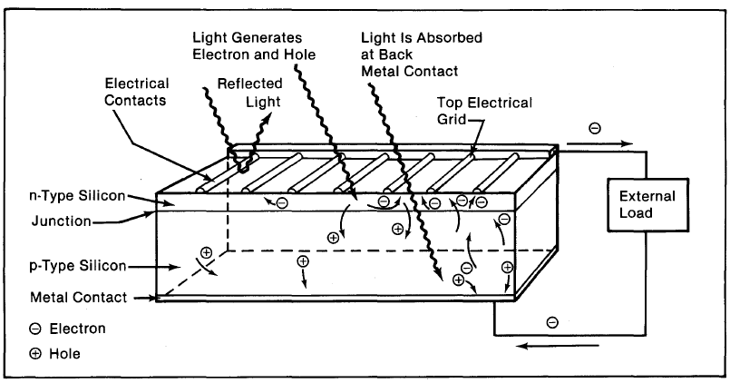
Figure 2-8. Light incident on the cell creates electron-hole pairs, which are separated by the potential barrier, creating a voltage that drives a current through an external circuit.
THE ELECTRIC CURRENT
If we connect the n-type side to the p-type side of the cell by means of an external electric circuit, current flows through the circuit (which responds just as if powered by a battery} because this reduces the lightinduced charge imbalance in the cell. Negative charges flow out of the electrode on the n-type side, through a load (such as a light bulb}, and perform useful work on that load (such as heating the light bulb's filament to incandescence}. The electrons then flow into the p-type side, where they recombine with holes near the electrode (Figure 2-8). The light energy originally absorbed by the electrons is used up while the electrons power the external circuit. Thus, an equilibrium is maintained: The incident light continually creates more electron-hole pairs and, thereby, more charge imbalance; the charge imbalance is relieved by the current, which gives up energy in performing work.
The amount of light incident on the cell creates a nearproportional amount of current. The amount of energy it takes to raise an electron to the conduction band is the amount of energy the light originally imparts to the electron and is, thus, the maximum that can be retrieved from the electron in the external circuit.
We have observed all the conditions necessary for current to flow: incident light to free the charge carriers, a barrier to accelerate the carriers across the junction and keep them at opposite ends of the cell, and a charge imbalance to drive a current (charged carriers) through a circuit.
BIBLIOGRAPHY
Backus, Charles E. (ed.}. 1976. Solar Cells. New York, NY: IEEE Press.
Chalmers, Bruce. 1976. "The Photovoltaic Generation of Electricity." Scientific American. Vol. 235 (No.4): pp.34-43.
Johnston, W.D., Jr. 1980. Solar Voltaic Cells. New York, NY: Marcel Dekker, Inc.; pp. 19-51.
Meinel, Aden B.; Meine], Marjori P. 1976. Applied Solar Energy. Reading, MA: Addison-Wesley Publishing Co.; pp. 526-544.
Noll, Edward M. 1975. Wind/Solar Energy. Indianapolis, IN: Howard W. Sams and Co., Inc.; pp. 7-44.
Pulfrey, David L. 1978. Photovoltaic Power Generation. New York, NY: Van Nostrand Reinhold Co.; pp. 66-113.
Tauc, Jan. 1972. Photo and Thermoelectric Effects in Semiconductors. New York, NY: Pergamon Press; pp.90-129.
Chapter 3
Physical Aspects of
Solar Cell Efficiency
HIGHLIGHTS
Most of the energy that reaches a cell in the form of sunlight is lost before it can be converted into electricity. Maximal sunlight-to-electricity conversion efficiencies for solar cells range up to 30% (and even higher for some highly complex cell designs), but typical efficiencies are 10%-15%. Most current work on cells is directed at enhancing efficiency while lowering cost. Certain physical processes limit cell efficiency-some are inherent and cannot be changed; many can be improved by proper design.
The major phenomena that limit cell efficiency are:
- Reflection from the cell's surface
- Light that is not energetic enough to separate electrons from their atomic bonds
- Light that has extra energy beyond that needed to separate electrons from bonds
- Light-generated electrons and holes (empty bonds) that randomly encounter each other and recombine before they can contribute to cell performance
- Light-generated electrons and holes that are brought together by surface and material defects in the cell
- Resistance to current flow
- Self-shading resulting from top-surface electric contacts
- Performance degradation at nonoptimal (high or low) operating temperatures
REFLECTION
Some of the sunlight that strikes a solar cell is reflected. Normal, untreated silicon reflects 36% (or more) of the sunlight that strikes it. This would be a horrendous loss in terms of efficiency. Fortunately, there are several ways of treating cell surfaces to cut reflection drastically. Among them are chemically coating and texturing the surface (these are covered in some detail in the next chapter). By dint of these methods, reflection can be lowered to a quite manageable 5% or so.
LIGHT WITH TOO LITTLE OR TOO MUCH ENERGY
Effects (2) and (3) are closely related: Efficiency losses are associated with light that either is not energetic enough (2) or too energetic (3) for the proper generation of an electron-hole pair. As stated in Chapter 1, sunlight has a varied spectrum; light reaching the earth has widely differing intensities at a broad spectrum of wavelengths. Losses associated with effects (2) and (3) result from how the light of varying wavelengths interacts with the solar cells.
Light entering a solar cell can (Figure 3-1)-
- Go right through it
- Become absorbed, generating heat in the form of atomic vibrations
- Separate an electron from its atomic bond, producing an electron-hole pair
- Produce an electron-hole pair but have an excess of energy, which then becomes heat
Only (c) is a near-perfect means of transforming sunlight into electricity.
At an energy that is specific to the material and its atomic structure, light can free an electron from its atomic bond (c) rather than just cause that bond to vibrate. Different solar cell materials have a different characteristic energy at which electrons are freed (socalled electron-hole generation).
For silicon, the energy is 1.1 electron volts;* for gallium arsenide, another cell material, it is 1.4 electron volts; other usable cell materials have characteristic energies ranging from 1 to 2.6 electron volts. This characteristic energy is called the material's band gap energy (the gap between the valence and conduction bands).
*An electron-volt is a measure of very small energies appropriate to atomic sizes. One electron-volt is the kinetic energy (energy of movement) an electron gains when it is accelerated by one volt of electric potential. which is slightly less than the voltage from a common flashlight battery.
Since the sun's spectrum has a wide variety of energies and intensities, the key is to match a material and its characteristic band gap energy with the spectrum so that the maximum amount of energy in the sun's spectrum falls just above the characteristic energy. Figure 3-2 shows how efficiency varies with the energy needed to generate an electron-hole pair. Notice that the energy required to free electrons in gallium arsenide, at 1.4 electron volts, nearly coincides with the peak efficiency associated with the spectrum; silicon, at 1.1 electron volts, is just below the peak efficiency.

Figure 3-1. What happens to light entering a cell? It can go through (a), can be absorbed as heat (b), can generate an electron-hole pair (c), or can generate an electron-hole pair and have excess energy that is lost as heat (d).
These estimates of efficiency assume effect (d), where light with energy greater than that needed for electronhole generation frees an electron but has excess energy that also produces heat.
The production of electron-hole pairs is essential to the working of a solar cell. Without it, no voltage can be generated and no current can flow. Effects (a) and (b) mentioned above are a total loss; effects (c) and (d) produce free electrons and holes, although some of the incident light's energy becomes heat in (d). Overall, these inefficient interactions of light with the cell material waste about 55% of the energy from the original sunlight. They are the largest single reason conventional solar cells cannot produce electricity with an energy equivalent to that from the sunlight falling on the cell. For comparison, consider how much more efficient solar cells would be if the sun's spectrum consisted of just one wavelength (monochromatic) and that was matched exactly to the energy the cell required to generate electron-hole pairs!*
*Such near-100% conversion of incoming light is the research goal of several projects in which sunlight is processed by various devices to make it monochromatic-however, investigation of these devices is beyond the purpose of this text.
Figure 3-2. Maximum efficiency calculated as a function of the energy needed to free an electron, assuming the outer space solar spectrum (AMO) incident on the cell and assuming a terrestrial solar spectrum (AM1); several semiconductors of interest are indicated (Cheremisinoff and Dickinson, 1980, p. 500).
RECOMBINATION OF ELECTRON· HOLE PAIRS
Loss mechanisms (4) and (5) result from the inadvertent recombination of electrons and holes before they can contribute to an electric current. Typically, these are small losses, because cells have been carefully designed to eliminate them.
Recombination of electrons and holes occurs in two ways, which can be characterized as direct and indirect recombination.
Direct Recombination
Direct recombination is relatively rare. It happens when an electron and a hole randomly encounter each other, and the electron falls back into the hole. Thus the material's original bonds are reasserted (Figure 3-3), and the electron's and hole's energies are lost as heat.
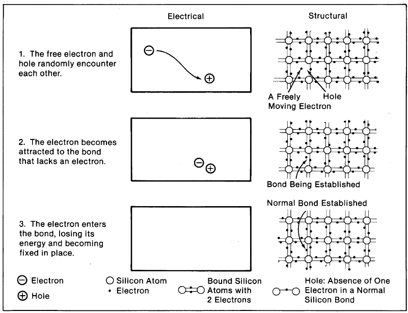
Figure 3-3. Direct recombination of an electron and a hole occurs randomly when an electron is near an empty bond. When the electron falls into the bond, it loses the energy it picked up from the light that freed it. This energy becomes heat.
Direct recombination is a problem only before the light-generated charge carriers are separated by the PV cell's junction (see Chapter 2). Recall that on the n-type side of the junction there are a preponderance of free electrons; on the p-type side, a preponderance of mobile holes. When light generates an electron-hole pair on the n-type side, the hole is in immediate danger of being filled by one of the huge number of free electrons. Cells must be designed to minimize the time the holes spend on the n-type side before they can be moved to the p side by the junction field. But once a hole reaches the p-type side (where it can contribute to an effective voltage) it is in relatively little danger of encountering free electrons, which are rare on the p-type side. The same argument can be applied to electrons generated by light on the p-type side; they must quickly be shuttled over to the n-type side to avoid recombination.
Indirect Recombination
Indirect recombination can occur in many ways. ("Indirect" means that the electron and hole do not just run into each other and combine-the interaction is influenced by further circumstances.) Contrary to what one might expect, indirect recombination is much more of a problem in solar cells than direct recombination. Experiment has shown that electrons and holes are lost via recombination in about a hundredth of a second, on average. (This gives an idea of how fast charge carriers must be separated by the junction in actual cells.) Calculations show that the direct recombination of an electron and hole would take place in about 1 second-one hundred times slower than actual measured recombination rates (Tauc, 1962, p. 69). Thus indirect recombination is dominant, causing a hundredfold increase in the recombination rate. The actual mechanisms of indirect recombination are manifold.
In the bulk of the material, recombination may be caused by empty, or dangling, bonds from impurities or defects (fractures), which can capture free electrons or holes.
Another recombination mechanism occurs when a free charge carrier has a collision, reducing its energy and raising the likelihood that it will fall into a bond. This is related to the intrinsic resistance in the cell (see the next section): More resistance reduces charge mobility, causing more recombination and less current and voltage.
The surface of a solar cell can be the site of much recombination. Minute "bridges" crossing the junction can exist on the cell's surface, giving the charge carriers a path that effectively avoids the junction's field. Charge carriers then filter back across the junction (in the opposite direction to junction-directed flow), diminishing cell voltage and current. Surfaces are also notoriously prone to unconventional atomic structures with numerous sources of collision and with dangling bonds; as such, they are regions where electrons and holes have many opportunities to recombine.
RESISTANCE
Resistance to the flow of current (i.e., the flow of electrons and holes) occurs in any electric circuit. We are most familiar with it from Ohm's law, V = JR, which can be rewritten as:
R = V/I,
where V is voltage, I is current, and R is resistance. This law is only true for certain materials at certain temperatures and currents. (It is not true for solar cells because recombination losses are not proportional to resistance.) Resistance is ever-present in most electrical elements, where the flow of current is accompanied by collisions between charge carriers and the material the charges are flowing through. Electric resistance can be so great that it can be used to provide heat (stoves) or light (light bulbs). Thus, resistance losses in cells are equivalent to energy losses; whatever a solar cell loses because of resistance degrades its efficiency.
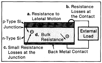
Resistance losses in solar cells occur predominantly in three places: in the bulk of the base material, in the narrow top-surface layer typical of many cells, and at the interface between the cell and the electric contacts leading to an external circuit (Figure 3-4). Resistance losses lower voltage and enhance the chances of recombination of charges, reducing current. Usually it is better to highly dope silicon to reduce resistance: Highly doped silicon has numerous free carriers to conduct the current. However, there are limitations associated with doping. Lattice damage can occur, and eventually there can be so many free carriers that the junction is defeated. (This is similar to the high temperature effect, see below.)
Figure 3-4. Most pn-junction cells have a very thin top layer. Just as resistance to water's flowing in a pipe is large for a narrow pipe, so is the resistance to lateral current flow large for electric charges in this thin top layer (a). Similarly, resistance losses are large at the electric contact (b), because of the poor interface between materials where disruptions in the atomic structure obstruct movement of charge carriers. There is even some (but very little) resistance loss at the junction (c) where the carriers, although accelerated, may lose some energy. The bulk of the material also has a resistance (d).
A representation of recombination and resistance losses can be seen in Figure 3-5.
Figure 3-5. The current and current losses of a solar cell can be modeled by a simple circuit with a current generator (J), a loss of current from recombination effects (Jr) resistance losses (R), and a shunt loss from current that returns across the junction (Rsh). Note that Jr reduces the current (arrows) reaching the external load, as does the path through Rsh (which would be optimized if it were infinite, i.e., no current could return across the junction). The resistance (R) blocks the flow of current, reducing voltage to load proportionately.
SELF-SHADING
Self-shading (7), like reflection (1), is one of the more obvious loss mechanisms in cells. It refers to losses engendered by the electrical grid on top of the cell, which reflects light that otherwise would enter the cell. Since resistance is maximal to lateral movement in the top-surface layer of the cell, there must be many charge removal points to minimize resistive effects. Thus electric contacts are not placed far from the charge carriers. The result is a grid-like geometrynarrow fingers of conductive material spread over the front surface of the cell. This electric grid shades a portion of the cell's top surface: A typical shading loss percentage is 8%, but some cells have losses as high as 20% and others as low as 3% (and less).
PERFORMANCE DEGRADATION AT NON-OPTIMAL TEMPERATURES
Solar cells work best at certain temperatures, according to their material properties: Some materials are more appropriate for use in orbit around the earth, some for terrestrial uses, and others for hightemperature applications either under concentrated sunlight or in space near the sun. Figure 3-6 shows how different cell materials lose efficiency with increasing temperature. Note that at normal terrestrial temperatures, 25oC, silicon's efficiency compares favorably with other materials; but at high temperatures, 200oC for instance, silicon's efficiency has dropped to 5%, whereas the other materials are near 12%. Silicon is a good material for ambient temperature terrestrial uses; it fails in high-temperature applications.
Although Figure 3-6 does not show it, there is a similar drop-off of efficiency below a certain low temperature for each of the materials.
Figure 3-6. Solar cells efficiency versus temperature for various materials: Note that all materials lose efficiency in the range shown.
High-Temperature Losses
The physical effects that determine efficiency's relationship with temperature are quite complex. For the most part, two predominate in causing efficiency to drop as temperature rises: As thermal energy increases, (1) lattice vibrations interfere with the free passage of charge carriers and (2) the junction begins to lose its power to separate charges. The first effect severely degrades silicon's performance even at room temperatures (Figure 3-7). The second effect does not occur until temperatures of about 300oC for silicon are reached. At such temperatures, a huge number of electrons in normal silicon bonds are thermally jostled from their positions; on the n-type side, they join and greatly outnumber the free electrons donated by the n-type dopant. At the same time holes are formed on the n-type side (left behind by the thermally freed electrons); the n-type silicon begins to lose its n-type character as the number of free electrons and holes become similar. The same process is working on the p-type side, which is losing its p-type character. This leads to two effects: (1) The thermally agitated charge carriers have so much energy, they cross over the junction in both directions almost as if the barrier field were not there. (2) Ultimately the junction itself disappears because there are no longer n- and p-type sides to induce it. All of these effects accumulate to erode the activity of the cell, and efficiency diminishes to nearly zero.
Figure 3-7. The ability of charge carriers to move without losing their energy is measured by their mobility, here shown for silicon (doped at two different donor concentrations) in relation to temperature. Note that silicon is already below its maximum efficiency at room temperature. The hightemperature losses shown here are mostly due to collisions with thermally excited atoms.
Since solar cells are sensitive to temperature increases, and since so much of the light energy incident on cells becomes heat (due to inefficiencies), it is frequently necessary to either match the cell material to the temperature of operation or to continually cool it, removing the extra, unwanted heat. Sometimes this latter method can lead to positive results, actually raising a solar installation's overall efficiency if the heat is applied to useful purposes (see Chapter 6).
Low-Temperature Losses
Low-temperature losses are, if anything, more complex and less understood. (They are important, however, only for deep-space PV applications.) Two effects are thought to play roles: (1)As temperature falls, thermal energy is less able to free charge carriers from either dopant atoms or intrinsic silicon. Mobility for light-generated charge carriers drops because they collide more frequently with ionized donors or acceptors in n- and p-type regions, respectively. The donors and acceptors are not screened as much by clouds of thermally aroused charge carriers. Also (2) at very low temperature, there is so little thermal energy that even dopants behave as if they were normal silicon atoms. For instance, in the n-type material, donor atoms retain their extra electrons; in the p-type material, holes remain fixed in place because electrons are less likely to pop out of their normal positions to fill them. Since the n- and p-type sides no longer exhibit their doped character, the junction disappears. (Recall that a junction forms only in response to imbalanced donor/acceptor concentrations.)
BIBLIOGRAPHY
Cheremisinoff,Paul N.; Dickinson, William C. (eds.). 1980. Solar Energy Technology Handbook, Part A. New York, NY: Marcel Dekker, Inc.; pp. 483-515.
Grove, A.S. 1967. Physics and Technology of Semiconductor Devices. New York, NY: John Wiley and Sons.
Meinel, Aden B.; Meinel, Marjorie P. 1976. Applied Solar Energy. Reading, MA: Addison-Wesley Publishing Co.; pp. 526-550.
Pulfrey, David L. 1978. Photovoltaic Power Generation New York, NY: Van Nostrand Reinhold Co.
Sutton, George W. 1966. Direct Energy Conversion. New York, NY: McGraw-Hill Book Co.; pp. 1-37.
Wolf, M. 1976. "Limitations and Possibilities for Improvement of Photovoltaic Solar Energy Converters." Solar Cells. Charles E. Backus (ed.). New York, NY: The Institute of Electrical and Electronics Engineers, Inc.; pp. 118-135.
Wolf, M. 1976. "A New Look at Silicon Solar Cell Performance." Solar Cells. Charles E. Backus (ed.). New York, NY: The Institute of Electrical and Electronics Engineers, Inc.; pp. 191-201.
Chapter 4
The Typical Single-Crystal
Silicon Solar Cell
HIGHLIGHTS
Single-crystal silicon is the most frequently used, bestunderstood material for solar cells. Knowledge of silicon's electrical properties and expertise with its manufacture have been gained in the transistor industry and in the solar cell industry, which has supplied arrays for generating power in space for over two decades.
Silicon does not exist in a single-crystal form in nature. Rather, it exists as silica, or silicon dioxide (SiO2), a compound of the two most abundant elements in the earth's surface. (Almost 60% of the earth's crust is silica.) A material called quartzite, which can be almost 99% silica in high-grade mineral deposits, is the usual starting point for producing silicon for solar cells. Other materials with a large amount of silicon-such as sand-are not good raw materials because they have too many impurities, which are costly to eliminate. Given the relative abundance and inexpensiveness of quartzite, it is clear that silicon is an attractive solar cell material.
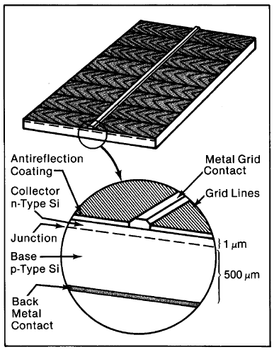
A typical pn-junction single-crystal silicon solar cell has several layers (Figure 4-1): a conducting grid on the top surface; an antireflective coating and/or treated surface layer; a thin layer of usually n-type silicon about one micrometer thick (called the collector); a very narrow junction-field region where there are almost no free charge carriers; a silicon base layer, oppositely doped to the collector (usually p-type); and a back-contact electrode. This chapter describes how each of these cell features is made and its practical functioning.
MAKING THE BASE LAYER
To make a solar cell, the starting raw material, quartzite, which is 90% or more silica (SiO2), must be refined and its impurities removed. The process begins when the quartzite is heated in the presence of carbon. This breaks the SiO2 into elemental silicon (Si) and carbon dioxide (C02). The silicon, however, still retains impurities originally in the quartzite. To remove most of these, an appropriate chemical vapor is blown over the silicon; the gas reacts with such impurities as aluminum, carbon, and magnesium, and they leave as part of the gas. After this process, the silicon still retains some impurities bad for a photovoltaic cell, so it is converted to a liquid called trichlorosilane (SiHCI3) using hydrogen chloride and a copper catalyst. The final purification of the silicon is then accomplished when trichlorosilane is distilled (much as are petroleum products), separating the SiHCl3 from the last impurities. Finally, the compound SiHCl3 is broken down and the pure silicon isolated by a slow, expensive, energy-intensive "chemical vapor deposition method" in which vaporized trichlorosilane is reacted with hydrogen gas, precipitating silicon. In total, this involved procedure raises the cost of silicon to about $70/kg; about 80% of this cost occurs in the last process, reducing trichlorosilane to a high-grade silicon.
Figure 4-1. A typical single-crystal silicon pnjunction solar cell.
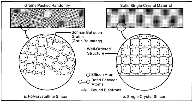
Figure 4-2. Purified silicon (a) is usually polycrystalline: It is made up of numerous single-crystal grains and electrically inhomogenous areas between them called grain boundaries. Single-crystal silicon (b) is structurally uniform and its electrical behavior is well understood.
This kind of silicon is a polycrystalline material (Figure 4-2a); that is, it is made up of numerous randomly packed "grains" of single-crystal silicon. To make effective solar cells, polycrystalline silicon must be processed into large-grained or single-crystal material (Figure 4-2b), the material used in the typical cell's base layer.
Making Single-Crystal Silicon
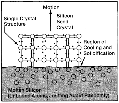
To turn polycrystalline silicon into single-crystal silicon, it must be melted and allowed to solidify in such a way that the silicon atoms arrange themselves in a perfect lattice (see Figure 4-2 and Chapter 2). This will happen naturally if the atoms of silicon are given time as they solidify to find their preferred positions (as opposed to being rapidly frozen wherever they happen to be). In general, the procedure is to cool the molten silicon very slowly while it is initially in contact with a single-crystal "seed" of silicon (Figure 4-3)
As the single-crystal silicon is grown, appropriate substances, or dopants, are introduced to make the base material behave electrically in the way necessary for solar cell operation. There are a number of dopants that can be used, but, in general, single-crystal silicon technologies have been developed for one combination -boron dopant in the base, phosphorus in the collector layer. (See Chapter 2 for the characteristics of these dopants.) Boron atoms can be introduced into the molten silicon before it solidifies as single-crystal material. As the silicon solidifies, the boron (acceptor) atoms assume places in the crystal structure that otherwise would be taken by silicon; this is the process whereby the silicon takes on its p-type electrical properties. A concentration of about 1016 atoms of added boron dopant per cubic centimeter exists in the final single-crystal material. This is about one boron atom for every million silicon atoms.
Figure 4-3. Molten silicon, solidifying in contact with a "starter" single-crystal seed, "grows" in a uniform manner, extending the single-crystal.
The above is a conceptual outline of single-crystal growth; but actual crystal growth takes many forms, each requiring different equipment and procedures. The two most established and dependable means of growing single-crystal silicon are the Czochralski process (Figure 4-4a) and the floating-zone technique (Figure 4-4b).
Figure 4-4. Converting polycrystalllne silicon to single-crystal silicon: (a) Czochralski growth apparatus and (b) floating-zone process.
The Czochralski Process. Here, a seed of single-crystal silicon contacts the top of a molten mass of purified silicon. The seed crystal is slowly raised (less than 10 centimeters per hour) and rotated. As the crystal rises imperceptibly from the melt, silicon freezes on its surface, extending the single-crystal structure. The final product is a cylindrical ingot, or "boule," typically 7.5 centimeters in diameter and many times that in length.
Controlling impurities is always a prime concern in making solar cells. In the Czochralski process, there are three processes that need to be managed:
- A wanted impurity, usually boron, is introduced in the molten silicon-it must be successfully transferred to the single-crystal silicon ingot.
- Unwanted impurities exist in the molten silicon, despite efforts to remove them during the previous purification steps-these unwanted impurities must be kept out of the crystal.
- The molten silicon is very susceptible to impurities that dissolve in it-especially those in contact with it because of the silica (SiO2) crucible holding the melt.
One reason that Czochralski-grown silicon is and has been a good material for solar cells is that the process naturally segregates impurities: that is, residual impurities in the molten mass of silicon tend to stay there rather than be incorporated into the crystal. (The large volume of molten silicon near the freezing region helps keep the impurities in the melt.) On the other hand, boron, which is the impurity that is needed for the cell to operate, is not segregated (as much) during Czochralski crystal growth; this felicitous behavior is the reason boron is most often chosen as a p-type dopant for silicon cells. One drawback of the Czochralski process, however, is that the SiO2 crucible in which the molten silicon is held loses some oxygen to the silicon, and this oxygen tends to move into the crystal in small, somewhat deleterious amounts. Also, at the end of each crystal "pull," the crucible cracks; a new pull requires a new crucible, adding to the process' cost.
The Floating-Zone Technique. This procedure requires an ingot of polycrystalline silicon and a seed crystal of single-crystal silicon. The polycrystalline ingot is placed atop the seed crystal and heated, causing the interface between the materials to become molten. While the ingot remains stationary, the heating coils are slowly raised. Single-crystal material solidifies below the molten interface and perpetuates upward as the heating coils move up. The technique is called "floating zone" because the region of molten silicon is unsupported; it maintains itself only by surface tension. The heating coils may be cycled up and down several times to assure total crystal uniformity, but this is not necessary for PV applications.
As with the Czochralski process, impurities are a concern with the floating-zone method. One relative disadvantage of the floating-zone technique is that it is less able to segregate impurities than the Czochralski process because the volume of molten silicon in which the rejected impurities are mixed is much less in the floating zone. On the other hand, the floating zone itself is not exposed to a silica (SiO2) crucible.
Making Wafers
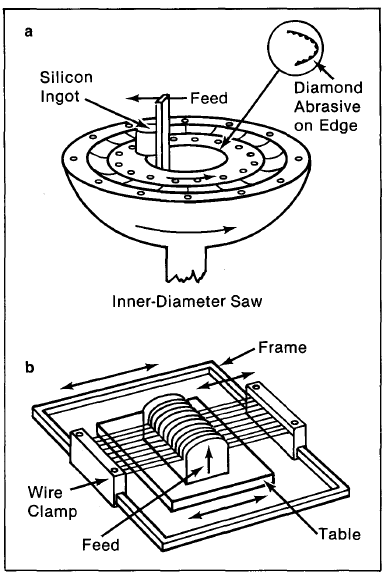
Once ingots of single-crystal silicon have been made, they must be cut and processed into wafers, which then form the base layers of solar cells. The first step is to mill the ingot so that it is uniformly symmetric; this may take a few millimeters off the typically 7.5-centimeter-diameter ingot. The next step is to cut the ingots cross-sectionally with diamond saws (Figure 4-5a) or multiwire saws (Figure 4-5b). Wafers are typically 0.5 millimeters thick; unfortunately, saws are also about this thickness, so almost half the single-crystal material is lost during slicing. The wafers are then polished to diminish small-sized surface defects, which would otherwise interfere with light-generated charge carriers and diminish the cell's efficiency.
This completes an overview of the fabrication of a typical cell's base layer. Clearly, fabrication is an expensive, complex process. As we will see in the next chapter, much research and development is being done to simplify it and lower its costs.
Figure 4-5. Schematic of (a) innerdiameter saw, and (b) multiwire saw.
FORMING THE pn JUNCTION
Conceptually, a pn junction is formed when a layer of doped silicon is brought in contact with an oppositely doped base layer of silicon. In practice, the procedure is somewhat different. In our typical cell, for example, an n-doped surface layer is formed by coating the top of the base layer with phosphorus and heating (but not melting) the surface, which allows the phosphorus atoms to diffuse into the silicon. The temperature is then lowered, the rate of diffusion dropping to zero. The region in which the phosphorus penetrates becomes an n-type collector layer. Below the n-type layer is a very narrow transition region in which the dominant dopant switches from phosphorus (n-type donor) to boron (p-type acceptor)-this is the junction. Below this, the p-doped base material is unchanged, maintaining its p-type electrical character.
Figure 4-6 shows how the concentration of phosphorus varies as the phosphorus atoms diffuse into the silicon at 950oC. The concentration of the boron atoms in the base is about 1016 atoms per cubic centimeter. Enough phosphorus is coated on the surface to have a concentration of about 1021 atoms per cubic centimeter there. Heating the surface layer causes the phosphorus atoms to penetrate the base layer, but the concentration naturally drops off with depth There are 1018 atoms of phosphorus per cubic centimeter at a depth of 1.2 micrometers into the material, two orders of magnitude more than the concentration of boron atoms there. Thus the n-type character of the silicon extends to 1.2 micrometers. Below 1.2 micrometers is the junction region. Further into the cell, the base material maintains its p-type electrical behavior.

Figure 4-6. Four diffusion profiles for 950oC diffusions of phosphorus into silicon. Timing (10, 20, 30, or 60 minutes) can be regulated to produce the right amount and depth of dopant. The base layer doping is 2 × 10¹⁶ boron atorms/cm3. The model cell (above, right) shows that the junction region is located where the toplayer doping and the base-layer doping are equal.
Note the very high concentration of phosphorus at the surface. The number of phosphorus atoms there is about a hundredth of the number of silicon atoms. Given this situation, the phosphorus atoms no longer assume places in the silicon crystal-there are just too many phosphorus atoms present for this simple structure. Instead, the phosphorus and silicon form an alloy, eliminating the donor-type electrical behavior of the phosphorus atoms. Because of this, the heavily doped surface shows little resemblance to n-type silicon: It is highly resistive and causes much recombination. Called the "dead layer," it is the subject of much work to minimize its negative effects.
The thickness of the top, collector layer is of some importance. Solar cell efficiency is aided when light generates electrons and holes near the junction because then there is more likelihood that these charge carriers will be separated by the junction. As an illustration, consider this possibility: If the top surface is too thin, almost all the light will pass through it and be absorbed below the junction. On the other hand, if the front surface is properly designed, it can be made the right thickness to absorb about half the light, while the remaining light can be absorbed on the other side of the junction; this would minimize the average distance from the junction of the light-generated charge carriers. * All of this is oversimplified but suggests the parameters involved in designing a cell's front layer. In silicon, light absorption depends on wavelength (shorter wavelengths are absorbed more easily): Over 50% of the sunlight incident on silicon is absorbed within 3 micrometers of the surface, but it takes almost 300 micrometers in total to absorb all the rest of the sunlight. This would suggest a cell with a shallow junction (less than 3 micrometers), a thick base, and a high mobility of charge carriers in the base (because light-generated carriers may be formed far from the junction).
*Each incremental thickness of silicon has a certain constant probability of absorbing light and having an electron-hole pair generated. The thicker the substance, the more likely light will be absorbed.
ANTIREFLECTIVE COATINGS AND ELECTRICAL CONTACTS
A surface through which light passes has to be treated so that it reflects minimally, and electrical contacts have to be attached to a cell to collect charges.
Untreated silicon reflects more than 30% of the light incident on it. However, a measured layer of silicon monoxide (SiD), a very good antireflective coating, can easily be formed on a silicon cell. A single layer of SiO reduces a silicon cell's surface reflection to about 10%, while a double layer (with another substance) can reduce it to below 3%.
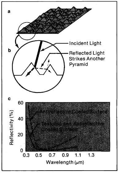
A further means to reduce reflection is to texture the top surface of a cell (Figure 4-7). Texturing causes reflected light to strike a second surface before it can escape, increasing the probability of absorption. For example, light with an 80% probability of being absorbed on one bounce (and therefore a 20% chance of being reflected) has a probability of being reflected twice or (0.2) × (0.2) = 0.04; i.e., its probability of absorption has been raised from 80% to 96% by the textured layer.
Figure 4-7. Texturing a cell exposes the tetrahedral surfaces of the silicon crystal lattice (a). Light that strikes the cell nearly perpendicularly (b) can either be absorbed or reflected; if it is reflected, it will strike another surface and have another chance to be absorbed. Note also that light that is absorbed is bent at the treated surface, so that it penetrates the cell obliquely. Because light travels through the cell at an angle, the cell need not be as thick to absorb as much light. The lower reflectivity (c) and the longer length the light travels through the cell give about a 15% improvement in cell efficiency over smooth, uncoated cells.
Electrical contacts must be attached to a cell for the cell to be placed in an electrical circuit. Design issues associated with contacts are similar to those associated with coated and textured surfaces. It would be best to completely cover the cell surfaces, back and front, with contacts; this would minimize the resistance that charge carriers experience. But, obviously, covering a cell with an opaque, metallic contact would completely block out the light. Thus a tradeoff must be made between resistance losses and shading effects. It is usual to design top-surface contacts as grids, with many thin conductive fingers spreading to every part of the cell's surface. The grid fingers must be thick enough to conduct well but thin enough not to block light. Such a grid keeps resistance losses sufficiently low, while shading only about 10% of the surface. Grids can be expensive to fabricate and can cause dependability problems. To make top-surface grids, metallic vapors can be deposited on a cell through a mask, or they can be painted on via a screen printing method. Attaching the back-surface contact to a cell is frequently not as complex: the contact simply can be a metal sheet. However, new cell designs [for concentrated light, for instance) may require that light enter the cell from the front and back, so that the back of the cell has to be treated antireflectively and have grid contacts, also.
Experiments are being conducted on alternative grid designs [such as putting them only on the cell's back surface) and on finding transparent grid materials, both of which are among the options examined in Chapter 5 on advanced silicon cells.
BIBLIOGRAPHY
Hovel, Harold J. 1975. Solar Cells. New York, NY: Academic Press; pp. 181-190.
Johnston, W.o., Jr. 1980. Solar Voltaic Cells. New York, NY: Marcel Dekker, Inc.; pp. 53-72.
Pulfrey, David L. 1978. Photovoltaic Power Generation. New York, NY: Van Nostrand Reinhold Co.; pp. 124-129.
Ravi, K.V. 1977. Journal of Crystal Growth. Vol. 39: p. 1.
Sittig, Marshall. 1979. Solar Cells for Photovoltaic Generation of Electricity. Park Ridge, NJ: Noyes Data Corp.; pp. 35-79, 126-149, 190-239.
Chapter 5
Advances in Single-Crystal
Silicon Solar Cells
HIGHLIGHTS
Progress aimed at making silicon cells more costeffective has advanced along two related fronts: new fabrication procedures and innovative cell designs.
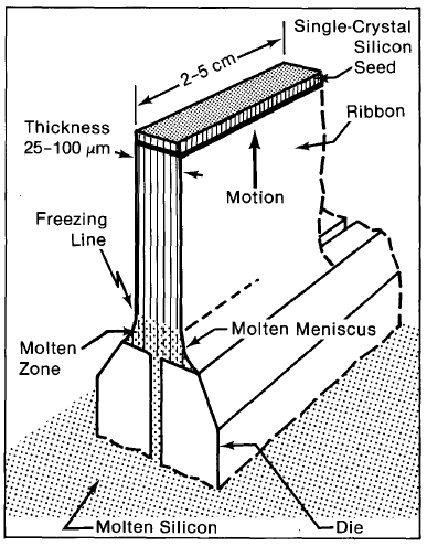
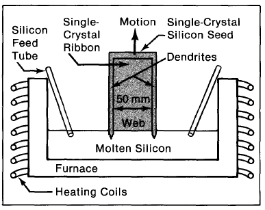
Single-crystal silicon technology is well developed. One strategy for reducing cost is to fabricate the cells less expensively by using less-refined silicon and by making silicon ribbons that can be made directly into wafers without excessive material losses due to cutting. Edge-defined film-fed growth, ribbon-to-ribbon growth, and dendritic web growth are among the processes that result in ribbons.
High-performance silicon cells incorporate several innovative features. Back-surface fields are built-in fields that reflect minority carriers toward the junction, raising output voltage, current, and efficiency. Similar fields can be used at the front surface.
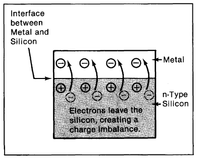
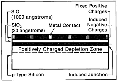
Schottky barrier cells are based on a junction effect that occurs at a metal-silicon contact. Their advantage is the elimination of the oppositely doped surface layer. Unfortunately, Schottky cells have exhibited less-than-adequate efficiency and are prone to degradation. Other designs that are being studied include metal-insulator-semiconductor (MIS) and semiconductor- insulator-semiconductor (SIS) cells, which are variations of the Schottky cell, and inversion layer cells.
Silicon cells for concentrated sunlight can be either single- or multijunction devices. Cooling is always necessary, since silicon performance drops rapidly with increasing temperature. Resistance losses are also critical; they are the main aspect attended to when designing a high-illumination cell. Grooved, multijunction cells have as much as 20% efficiency at 600 suns.
Other cell components and fabrication techniques are being researched. Laser-induced diffusion seems a promising alternative to thermal diffusion for junction formation. Antireflection layers are being optimized, especially via double layers and pyramidal texturing. Selective surfaces can lower heating effects. Polishing the back of a cell that has a textured front surface results in total internal light reflection, which allows cells to be thinner.
NEW FABRICATION
Silicon, as it is found in nature, is expensive to transform into single-crystal "wafers" for solar cells. Conventional methods for producing the material from which wafers are cut, the Czochralski and floatingzone techniques described in the previous chapter, "grow" single-crystal* silicon in ingots from molten silicon starting with single-crystal seeds; then the ingots are sawn into wafers. These are complex, expensive processes. New fabrication processes try to reduce expense by changing raw silicon into single-crystal silicon more cheaply, and by forming single-crystal silicon directly into usable wafers while avoiding steps such as sawing. Newer processes that incorporate this strategy by producing ribbons (long, thin, rectangular sheets) of single-crystal material include:
- Edge-defined film-fed growth (EFG)
- Dendritic web growth
- Ribbon-to-ribbon (RTR) growth
*The processes described in this chapter produce either single-crystal silicon or a similar material (large-grained polycrystalline silicon) with similar electrical properties. For purposes of simplicity, such material will simply be referred to as "single-crystal silicon."
Edge-Defined Film-Fed Growth (EFG)
One of the more promising methods of making single-crystal ribbons is edge-defined film-fed growth, In this process, highly pure, molten silicon is drawn upward by capillary action through a narrow, slotted mold of carbon or other appropriate material, producing a continuous single-crystal ribbon (Figure 5-1).
There are several problems associated with edgedefined film-fed growth. The die must be of a highly refined material that has the proper capillary characteristics and does not contaminate the silicon. So far, carbon has been the best die material, but it still introduces some impurities. This problem is exacerbated because there is very little volume (between the die and the single-crystal product) in which contaminants can dissipate; i.e., EFG does not retard impurities entering the ribbon from the melt as well as do some processes. Thus, to avoid contamination, a highly pure silicon melt must be provided as starting material. Additionally, repeated use tends to erode the die.
Figure 5-1. Edge-defined film-fed growth (EFG): A seed crystal of single-crystal silicon contacts the surface of the melt as it gets drawn through the die by capillary action. As the crystal is slowly raised (about 15 em/min), the silicon cools and freezes into a single-crystal ribbon.
EFG does not produce single-crystal silicon per se; because of impurities and stress resulting from process geometry, the ribbon has crystal lattice defects. For this reason, PV performance of cells made from EFG ribbon has not been as high as, for instance, with Czochralski-grown wafers. Cells from laboratorygrown ribbons have attained 12% efficiency. Raising the efficiency of EFG-processed cells is one of the high-priority goals of current work. This is mainly a matter of eliminating die contamination and resultant silicon defects. Success may make EFG a central process in future cost-effective silicon cell manufacture. .Projections (Backus, 1976, p. 395) are that EFG can be reduced in cost 10-100 fold, which is the amount needed to support overall goals for making PV generally cost-competitive.
Dendritic Web Growth
Dendritic web growth has yielded cells with efficiencies (about 15%) as high as any among the single-crystal silicon processes, notably Czochralski silicon; however, the cost of web growth has yet to drop to competitive levels.
Dendritic web growth (Figure 5-2) is similar to EFG, except the mold is eliminated. Twin single-crystal dendritic (wire-like) seeds are allowed to touch and grow slightly into molten silicon. As the dendrites are withdrawn, because of silicon's surface tension, a web of single-crystal silicon forms between them, solidifying as it rises from the melt.
Exact thermal control is essential to dendritic growth. There is a tendency for the web to thicken in the middle; any deviations in temperature from a precalculated optimum result in a poorly grown web.
Dendritic web growth avoids some of EFG's problems with the die (contamination and die erosion), but has several problems of its own, the main ones being a slow growth rate and the need for precise temperature control. Experimental growth has not yet exceeded about 2 em/min for wide (5-cm) strips. One parameter restraining high growth rate is that faster solidification lessens the process' ability to keep impurities in the liquid from entering the crystal. An inherent problem with the process is the dendrites: Because of their shape, they cannot be used for the final cell and have to be cut off. However, they can be melted down and used to grow new webs.
Figure 5-2. Dendritic web growth: A web of single-crystal silicon forms as dendritic seed-crystals are withdrawn from the melt.
Ribbon to Ribbon (RTR) Growth
Ribbon-to-ribbon (RTR) growth (Figure 5-3) is essentially the same as the floating-zone technique, except it is applied to ribbons of polycrystalline silicon feedstock rather than to cylindrical ingots.
A disadvantage of RTR is the need for a polycrystalline ribbon; also, there is a high-defect incorporation, especially if the process is speeded up to meet cost goals. Stable RTR growth rates of 7 em/min have been obtained. Cells with 13%-14% efficiency are typical of RTR growth. Work to generate high-quality polycrystalline silicon more cheaply or else to use less-refined material is underway. If such work succeeds, RTR may become a key process in making usable wafers.
Figure 5-3. Ribbon-to-ribbon (RTR) growth: An unsupported (floating) zone of silicon melted by a laser recrystallizes as a single-crystal ribbon.
In all the ribbon technologies, the aim is to go from a little-refined feedstock to an efficient solar cell as inexpensively as possible. Ribbons reduce or eliminate two costs: waste from slicing ingots into wafers and from cutting the wafers into rectangles (if it is done). Other processes that attain goals similar to the ribbon technologies are being looked at. They include cell fabrication from thin-film materials such as cadmium sulfide or amorphous silicon (a kind of non-crystalline silicon). The goal is to produce a cell that can be manufactured cheaply, in quantity, with little energy input, and with precise, reproducible quality.
INNOVATIVE CELL DESIGNS
Just like new fabrication techniques, new cell designs have the potential of raising efficiency and/or lowering cost. All cells work by the same principles: charge generation and separation causing photovoltage and current flow. But some cell designs are better than others.
Back-Surface Fields (BSF) and Other Minority Carrier Mirrors (MCM)
The main built-in field in a cell is at the junction, where the charge carriers that do all the work in a PV cell are separated. Building another electric field into a cell's structure can enhance efficiency. One way is to create a so-called back-surface field (BSF), a special case of a more general concept, the minority carrier mirror (MCM). Back-surface fields are built-in fields at the back of a solar cell that reflect minority charge carriers back toward the junction (Figure 5-4a). In pnjunction devices, minority carriers (electrons on the p-side, holes on the n-side) are generated by light and diffuse to the junction randomly, where they are sent over to the side of the cell where they are the majority carriers. This is the way charge separation and photovoltage occur. A back-surface field serves to keep the minority carriers from randomly striking the back of the cell, where they would reach an electrode and prematurely recombine. For instance, if an electron were moving randomly on the p-type silicon side and it were to reach the back electrode, it would recombine with the holes there, thus reducing charge separation and lowering the cell's output voltage. Instead, the BSF reflects electrons back toward the pn junction, where they are sent into the n-type side of the cell, enhancing the cell's carrier collection efficiency and thus its voltage and current.
The BSF is set up in a cell during its fabrication in much the same way as a pn junction. For instance, a BSF can be created in a typical cell that has a thin n-type silicon layer atop a thicker base layer of p-doped silicon by doping a thin layer (1 micrometer) of higher concentration p-dopant into the back of the cell (Figure 5-4b). This creates a cell having three layers: n on p on (so-called) p+ (the p+ indicates the higher concentration of p-type dopant). The p+ layer can be made in any of the ways the top n-type layer is made; i.e., boron (an acceptor, or p-type, impurity) can be precipitated on the back and can be caused to permeate the silicon by suitably raising the temperature. The BSF itself closely resembles a pn junction; it results from the same charge adjustment process that creates the pn junction (Figure 5-4c). For instance, the pp+ junction forms because a highly concentrated p+ region has many more holes than the nearby p-type silicon. Electrons therefore move over from the p region to fill nearby holes in the p+ material until they set up a repulsive field that prevents further electrons from moving over. It is this repulsion of electrons that is characteristic of the pp+ BSF structure. When the cell is exposed to light and electron-hole pairs are being generated on the p side, some electrons randomly head for the back of the cell. The BSF repels them, sending them toward the junction for effective use. Holes, on the other hand. go right through the BSF and reach the back electrode. where they recombine with electrons drawn from the external circuit (Figure 5-5).
A back-surface field can enhance a cell's output voltage by 10% (about an extra 0.05 volts) and raise a cell's efficiency by a few percent. Highly sophisticated cells for uses that demand high efficiency can also incorporate a minority carrier mirror at the front of the cell; for instance, an n+npp+ (where n+ indicates a higher concentration of donor dopant) cell would reflect holes from the front surface and electrons from the back. Unfortunately, artificially induced n+npp+ designs may be more expensive to fabricate than can be justified by their performance. However, sometimes natural front-surface minority carrier reflection takes place in cells due to the junction formation process. If ion implantation (see below) or thermal diffusion is used to fabricate the junction, the process creates an impurity concentration gradient similar to an n+n concentration. This acts to encourage the correct movement of carriers at the frontsurface of the cell.

Figure5-4. A back-surface field (a) reflects minority charge carriers back toward the junction, increasing the efficiency of charge separation. The high concentration of boron (acceptor) dopant in the npp + cell (b) creates the back-surface field (c).
Schottky Barrier Cells
A Schottky barrier cell is a solar cell whose junction is induced when a metal contact is applied to the surface of silicon that has been suitably doped. As a result of the electronic properties of silicon and metal, charge carriers are distributed at either side of the contact interface in a way that induces a built-in field just inside the surface of the silicon similar to that of a pn junction (Figure 5-6).
When light strikes the Schottky barrier cell, the electron-hole pairs are generated in the silicon. Holes then migrate into the metal contact, and electrons from the metal migrate into the silicon (assuming n-type silicon, as in the Figure); this causes a current to flow. The marked advantage of the Schottky cell is that it eliminates the top-surface, oppositely doped collector layer. Unfortunately, there are many problems with Schottky cells. The semitransparent metal contact on top cannot act as a conducting grid because it is too thin (resistance is too great). It is necessary to attach a grid on top of it, thus reintroducing shading effects and higher costs.
In fact, attaching grids has become one of the main stumbling blocks in the use of Schottky cells. The usual grid-attachment technologies require high temperatures, which damage a cell's top, metallic layer. Thus, new techniques have had to be developed. The thin metal layer is itself a serious problem, because the cell's performance is very sensitive to how well it is made. Slight fluctuations in quality of the metal-silicon interface lead to much lower electricity producing efficiencies. Perhaps because of surface de
gradation, Schottky cells have exhibited poor longterm reliability. They are especially prone to degradation in humid climates. On the whole, Schottky cells have not displayed the performance (their efficiencies are consistently lower than pn-junction cells), the reliability, or the low cost hoped for them, and there is serious doubt whether in their conventional form they will ever compete with pn-junction cells.
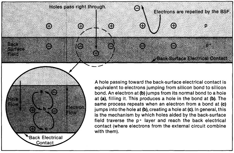
Figure 5-5. A BSF reflects electrons and is "transparent" to holes (a). A hole passing through the BSF is equivalent to electrons from silicon bonds moving to the left; at the electrode, the hole is filled by an extra electron that has moved through the external circuit (b).
Figure 5-6. Formation of a Schottky barrier cell: Electrons and holes at a metal-semiconductor interface redistribute themselves in much the same way they do when n- and p-type silicon are joined. The barrier then acts like a pn junction to separate charge carriers.
Two variants of the Schottky cell are being looked at as possible improvements. They are the so-called MIS (metal-insulator-semiconductor) and SIS [semiconductor- insulator-semiconductor) cells. These cells were discovered fortuitously. The layer of silicon oxide (an insulator) that naturally forms on the surface of silicon exposed to the atmosphere was found to help rather than hinder the voltage of a Schottky cell; l.e., a metal, silicon oxide, silicon (MIS) structure works better than a regular metal-silicon contact. The insulator is usually very thin (20 angstroms or less) so as not to impede the passage of current during illumination. A SIS cell replaces the thin transparent layer of metal on the surface of the cell with a somewhat thicker layer of heavily doped, conductive, transparent semiconductor such as indium tin oxide; this top layer acts just like the metal to induce the junction (in the oxide layer), but has the added advantage that it can be made thick enough to reduce substantially the need for a top-surface electrical contact without incurring resistance losses.
MIS and SIS cells have most of the problems of normal Schottky cells, especially quality control during fabrication (because of their thin but very electrically sensitive layers) and degradation during operation. As of now, MIS and SIS cells on single-crystal wafers are not very promising. (Results may be more favorable for polycrystalline and amorphous silicon materials.)
Inversion Layer Cells
A new: cell design with a high efficiency (currently 17%) and high voltage potential is the inversion layer cell. It has been found that a layer of SiO deposited on SiO2-coated p-type silicon induces a junction near the top of the p-type silicon (Figure 5-7). Vapor SiO loses electrons as it solidifies, causing the layer of SiO to have a positive charge. This positive charge pulls the few free electrons in the p-type silicon to the interface between the Si and SiO2, causing that region to behave as if it were n-type silicon. (The value of the insulating SiO2 layer is that it prevents these electrons from entering and neutralizing the SiO.) Since the layer just beneath the SiO2 becomes n-type and the bulk silicon is p-type, a pn junction is induced in the silicon. When the cell is illuminated, the junction separates electrons and holes just like a regular pn junction. (The lightgenerated electrons have enough energy to tunnel through the SiO2 and preferentially enter the metal contacts.)
Another variant of this design is to lightly dope the top of the p-type silicon with n-type dopant before applying the SiO2 and SiO. This aids carrier mobility (less resistance in the top layer) while enhancing the pn junction's voltage.
Figure 5-7. In an inversion layer cell, a junction is induced within p-type silicon by the presence of fixed positive charges in a top layer of SiO.
Advantages of these cells are the relative simplicity of handling SiO and SiO2; the induced junction within a relatively fault-free material (less doping means fewer lattice defects); and the potential for high voltage and efficiency.
Cells for Concentrated Sunlight
A major strategy for reducing the system cost of PV is to concentrate sunlight onto specially designed, highly efficient cells. Cell efficiency actually rises with illumination, and current is nearly proportional to illumination for quite high levels of intensity (Johnston, 1980, p. 160). Concentrating the sunlight one hundredfold, for instance, means that one-hundredth the number of expensive cells need be used. The tradeoff is the cost of the necessary light-concentrating (mirrors or lenses) and sun-tracking equipment needed for the high-intensity system (see Chapter 7).
High temperatures are a problem in concentrating systems since the high-intensity light creates more heat in addition to more PV current. Silicon cells perform poorly at high temperatures. To be used in concentrating arrays, silicon must be cooled to near-ambient temperatures.
A second physical parameter of importance in concentrating systems is resistance to current flow, especially in a cell's surface layer. Power loss in cells is proportional to the resistance times the square of the current. Since current is enhanced proportionally in high-concentration sunlight, power loss becomes very large, especially if resistance is not lowered to compensate. Two choices exist for reducing front-layer resistance. making the front layer thicker or making the contact grid more extensive. The latter is the usual choice, raising self-shading to about 10% (or more) in these cells. Despite high shading, concentrating cells using extensive grids have performed at high efficiencies (about 20%) under up to 1000 suns of illumination. *
*One sun is the energy (about 1 kW/m2 ) of sunlight striking the earth's surface; one hundred suns is the energy (100 kW/m2 ) of sunlight concentrated 100 times.
Cooled, specially optimized (with back-surface fields, minority carrier mirrors, etc.), single-junction silicon cells are appropriate for concentrations of less than 100 suns. Other more-costly designs are preferable above 1000 suns; these designs incorporate multijunction geometries. Two such will be looked at here: interdigitated back-contact cells and grooved-junction cells.
The Interdigitated Back-Contact Cell. This device, having no front contacts, avoids self-shading entirely (Figure 5-8).

Figure 5-8. Interdigitated back-contact cell: There is no top-surface grid and thus no self-shading.
In the interdigitated cell, the many small regions of highly doped p+ and nt-type silicon act as collectors of charge carriers-electrons moving into the n" -type, holes into the pt-type. The fields around the doped regions are set up similarly to other junctions (pn or Schottky) via the rearrangement of charge carriers. Charge carriers are generated by light in the bulk of the cell above the junctions; the bulk material is p-type silicon. The main advantage of the cell is the elimination of all self-shading; careful design of the doped regions can also lower resistance, which is important in concentrating systems. High performance (above 17% efficiency) has been attained, but as yet the cost of fabrication is noncompetitive.
The Grooved Junction Cell. This is a very effective design, with measured efficiencies of more than 20% at 600 suns. The main advantage is its low resistance near both front and back contacts. Charge carriers are also separated and collected with high efficiency because of the many, close-by junctions. Self-shading is high; for example, in the sample cell (Figure 5-9), shading is 20%. Other grooved geometries have lower shading but higher cost.
These are examples of multijunction geometries for single-crystal silicon. Many other possibilities are available for other kinds of silicon and other materials.
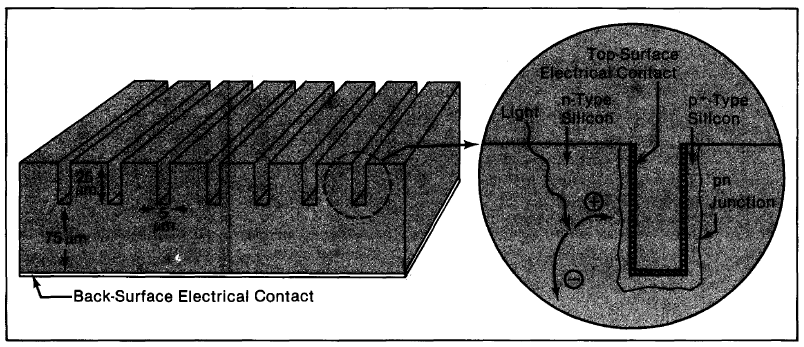
Figure 5-9. Grooved junction cell.
Advances in Component Technologies
The performance of each component of a cell can be optimized, e.g.,
- Alternate junction formation (ion implantation, laser diffusion)
- Grid technologies
- Antireflection technologies
- Back-surface light reflectors
Alternate Junction Formation. Problems with cost and control associated with high-temperature diffusion have led to work on other means of forming a surface layer and junction in a pn cell. One method, ion implantation, uses a high-energy beam of dopant such as phosphorus [n-type] to do the implanting. A properly doped p-type base material is exposed to a beam of phosphorus ions, which penetrate to an adjustable depth, depending on the strength of the beam. However, the beamed-in phosphorus donors do not readily assume places in the silicon lattice (necessary for proper electrical behavior) and their bombardment also tends to damage the lattice. Thus, it is usually common to "heal" the lattice, causing the phosphorus to become electrically active, by either heating the silicon or exposing it to a short (10-7S) burst from a laser beam. Once this is done, the junction and surface layer resemble a conventional diffusion-formed structure: Typical junction depth can be 0.25 micrometer and concentration of impurities varies from 1016 atoms/em3 at the junction to 1021 atoms/cm3 at the surface.
Ion implantation has several advantages (some of them still potential) over thermal diffusion. In general, despite the annealing step needed to heal the crystal, ion implantation uses less energy. The technique itself is simpler and more reproducible in large-scale operations. Because depth of junction and dopant concentration are somewhat controllable, more flexibility exists. Finally, thin-layer, highly doped back-surface fields can be formed on the cell simultaneously with the front-surface implantation. (Both can be healed in the subsequent heating or laser process.) Calculations performed for models of industrial-scale systems suggest that current technology can make ion-implanted junction cells very cheaply (Kirpatrick et al., 1980), making ion implantation a very promising technique for meeting desired cost goals.
Laser-induced diffusion is accomplished in a way similar to thermal diffusion: A layer of appropriate dopant is put on the surface of the oppositely doped base and then, instead of heating, a laser beam is applied causing the dopant atoms to diffuse into the silicon. Current work with laser-induced diffusion has resulted in cells with 10% or greater efficiency. The simplicity and effectiveness of the technique suggest that it may be part of the future fabrication of low-cost silicon cells.
Grid Technologies. Electrical contact is necessary for all cell performance, and its apparent simplicity belies the difficulties actually encountered. Characteristically, it is quite hard to fabricate a grid that is in good electrical contact with a cell and that will not degrade given temperature and/or humidity fluctuations. Typical contacts are made of three layers attached to the silicon: a layer (titanium) that makes a good contact; a layer (palladium) that can serve as a glue; and a final layer that is a good conductor, such as silver.
The nature of the top surface contact varies from no grid (for interdigitated, back-contact cells) to highly complex grids for cells used under concentrated sunlight (where high surface-layer electrical resistance is a problem). Typical grids are made with "fingers" leading from a bar along one side of the cell. Highly efficient grids require many narrow fingers (64 is not unusual), perhaps crossed, and perhaps thickening toward the bar for better conductivity.
Antireflection Technologies. Means of assuring low ref1ection of incident light are also being optimized. Coatings of silicon monoxide (SiO) and dioxide (SiO2) titanium dioxide (TiO2) and/or tantalum pentoxide (Ta2O5 are being used to reduce reflection. For singlelayer coats, SiO2 is favored (reducing reflectance to less than 10%). Double-layer coatings, though, are more effective: 600 angstroms of Ti02 and 1100 angstroms of SiO2 reduce reflectance to 3%.
Another possible strategy in deriving the most from the available light is to make a so-called selective surface that actually reflects unwanted light. For instance, light below a certain energy cannot create an electron-hole pair and is worse than useless to the cell (since it will become heat if it is absorbed). Using a selective surface to reflect low-energy light may be valuable for high-concentration cells, where heating effects are crucial.
Back-Surface Light Reflectors. Essentially, this method uses mirrors to reflect the light before it can leave through the back of a cell. Cells designed to take advantage of back-surface mirrors can be narrowed to about half their original thickness; in narrow cells, much light strikes the mirror but is reflected back into the cell for conversion. Narrowing helps improve collection efficiency, since the charge carriers are generated closer to the junction. But narrowing's major contribution is cutting the need for high-cost cell material.
A back-surface mirror can be made by inserting a narrow plane of aluminum between the cell and the back electrode. But special back-surface mirrors can be eliminated, and the effect maintained, by another strategy entirely: If the front surface is textured into pyramidal shapes for antireflection, it bends all incident light in such a way that it strikes a polished, but otherwise untreated back-surface of the cell obliquely. Light striking any inner surface (such as the surface of a pool, seen from below) at angles greater than a certain known critical angle (measured from the perpendicular) will be reflected back into the cell. (That is why you cannot see the sky from the bottom of a pool unless you look almost directly up.) Thus, texturing the front surface of a cell and polishing the back causes the light to be reflected back and forth within the cell (total internal reflection) until it is all absorbed, even if there is no back-surface mirror at all.
The fully optimized single-crystal silicon cell is the workhorse of the solar cell technologies. Different materials or cell designs may ultimately displace itor silicon may continue to be improved and remain the leader in terrestrial PV power generation.
BIBLIOGRAPHY
Backus, Charles E. 1976. Solar Cells. New York, NY: IEEE Press; pp. 191-299, 295-311, 393.
CNE8 (Centre National d'Etudes Spatiales), 1971. Cellules Solaires (Solar Cells]. New York, NY: Gordon and Breach Science Publishers; pp. 275-425.
Cheremisinoff, Paul N.; Dickinson, William C. (eds.) 1980. Solar Energy Technology Handbook, Part A. New York, NY: Marcel Dekker, Inc.; pp. 489-515, 517-540, 542-551, 556, 558.
Dixon, A.E.; Leslie, J.D. (eds.). 1979. Solar Energy Conversion. New York, NY: Pergamon Press; pp. 805817,820-: 826, 843-ffi5, 869-884.
Hovel, Harold J. 1975. Solar Cells. New York, NY: Academic Press; pp. 112-127, 139-148, 181-190, 199-210.
Johnston, W.D., Jr. 1980. Solar Voltaic Cells. New York, NY: Marcel Dekker, Inc.; pp. 36-39, 67-72, 95-102.
Kirkpatrick, A.R.; Minnucci, J.A.; Greenwald, A.C. 1980. "Low Cost Ion Implantation." 14th IEEE PV Specialists Conference-1980. New York, NY: Institute of Electrical and Electronics Engineers, Inc.; p. 820.
Maissel, Leon I.; GIang, Reinhard. 1970. Handbook of Thin Film Technology. New York, NY: McGrawHill Book Co.; Section 14.
Pulfrey, David L. 1978. Photovoltaic Power Generation. New York, NY: Van Nostrand Reinhold Co.; pp. 85-91, 97-99, 100-103, 124-141, 164-170.
Sittig, Marshall. 1979. Solar Cells for Photovoltaic Generation of Electricity. Parkridge, NJ: Noyes Data Corp.: pp. 36-67, 127-183, 190-240.
Williams, E.W. (ed.). 1978. Solar Cells. New York, NY: Institution of Electrical Engineers, Inc.; pp. 83-S40.
Chapter 6
Solar Arrays
HIGHLIGHTS
Individual solar cells have limited power and must be tied together electrically in order to produce enough electricity for most applications. In essence, cells need only be joined to. one another in progressive size levels until Jheir individual power contributions add to that fulfilling a designed need. In practice, certain electrical precautions must be taken in building to desired power levels so that if some cells fail they will not cause failure of an entire assembly. There are other, non-electrical considerations in producing a PV assembly. They include protection against the assembly's environment (temperature, precipitation, etc.), and waste heat within the assembly itself. Protection from the environment can be achieved by encapsulating. Heat can be transferred away from the assembly by convective, conductive, and radiative means. The heat can also be used for space heating or to produce electricity to supplement that produced by a PV system.
PV BUILDING BLOCKS
The effects discussed in previous chapters have demonstrated that producing electricity from photovoltaics is simple in theory but somewhat difficult at the practical level.
Under the best circumstances, single PV cells have limited output. Individual cells can be used to power small, power-miserly equipment such as toys, watches, and pocket calculators. But to provide reasonable power for many practical applications, voltage and amperage outputs from the PV source must be increased. On paper, this is easy: According to electrical principles, voltages and currents can be increased by suitably connecting power sources. In practice, however, increasing the power levels from photovoltaics is not straightforward and depends on many factors internal and external to the PV cells themselves.
Some of the factors that must be managed are the variability of individual-cell energy output (which can worsen with age) and potential problems with the integrity of the connections linking one cell to another. Besides these problems, which are tied to the cell itself, the designer grouping PV cells in a large terrestrial installation must account for uneven illumination-such as caused by cloud shadows, for example.
Boosting Voltage and Amperage
Ideally, connecting individual cells in parallel-that is, tying a common lead to all positive cell terminals and another lead to all negative terminals-under proper conditions can produce an amperage output from the group of cells that is the sum of that from the individual cells. (There is no voltage increase.) In a very real sense, combining cells in parallel is equivalent to making a cell larger.
Also under ideal conditions, when solar cells are joined in series-that is, when the positive lead from one cell is joined to the negative of the next, and so on-the voltage contibution from each adds. (The total current available from integrating the cells in this way is no more than from an individual cell.)
It is possible to gather cells into groups (parallel, current building) and then "string" the groups together (in a series, voltage-building configuration). Or it is possible to gather the cells by stringing them to build the voltage and then grouping the strings to increase amperage (Figure 6-1).
There are several structural levels associated with bringing solar cells together.
The first, most basic gathering of PV cells is the module, which may integrate fewer than a dozen cells to as many as 100 cells. At the next level is the panel, comprising groups (parallel connections) of modules and/or strings (the series connection of modules or groups). Next is the array, the combining of panels in series and/or parallel arrangements. Last is the array field-a composite of arrays.
If the electrical performance of each cell is the same, then it makes no difference how the strings and groups are ordered in achieving a desired output. Unfortunately, actual cells vary in quality: Even under like conditions of illumination, not all cells behave alike. Inherent cell-to-cell differences are aggravated by uneven illumination. Even worse, if some cells fail and lose their ability to function altogether, they may block current flow like an open electrical switch. Others break down and become, for all purposes, a simple connecting wire, short-circuiting a part or all of the array. At a minimum, such effects lead to reduced array output. At their extreme, such effects can cause the destruction of an array from overheating.
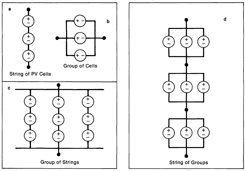
Figure 6-1. Voltage is boosted by stringing cells in a positive-to-negative-to-positive arrangement (a), while amperage is increased by grouping cells together in parallel (b) such that all positive leads are tied, as are all negative leads. Grouping strings together (c) or stringing groups (d) increases both the voltage and current.
The effect of such breakdowns and some other performance irregularities in a solar array can be minimized by inserting appropriate electronic components into the module circuitry. One precaution against single-cell breakdown affecting other areas of the module is to place solid-state diodes (devices that permit electricity to flow in a single direction) either in line with or across a string of cells at appropriate junctures. Placement depends on how the diode is to be used to protect the module (Figure 6-2). The use of diodes can cut into electric-energy output when all of the module's cells are properly functioning. In such cases they represnet an unwanted load. The designer must trade security (adding diodes) against a reduction in output performance.
Figure 6-2. Blocking diodes are used to avert failure,such as when a short-circuit fault occurs between adjacent strings of solar cells. Without the diodes, the primary bus would sustain severe damage.
Design Requirements for Connecting Components
Even with ideal cells capturing the sunlight from a cloudless sky, putting individual cells together can present challenges. The sheer numbers needed to build the power levels commonly associated with utility-plant output create design problems. Simply joining cells into a large enough matrix to provide 100 megawatts would create a PV system configuration measuring more than several square kilometers, including space between arrays and that for auxiliary equipment. The designer will be expected to confront electrical, mechanical, and other design considerations in putting together such a configuration.
THE PHYSICAL CONNECTION
Connecting cells and modules and arrays is an extremely important aspect of PV technology. The connections have to provide good conductivity and reliability for extended periods despite large temperature variations and other climatic variables that tend to disrupt and/or deteriorate electrical integrity.
Cells are usually built up into modules by attaching one to another with metal shaped from soild wire or solid or meshlike ribbons (Figure 6-3). The interconnection can be rigid or flexible, although it is usually flexible to contend with movement within the array produced by thermal expansion and other forces. (Early solar panels did not employ interconnecting aids, but contained cells electrically tied to one another by physically contacting the top of one cell to the bottom of a following cell. Failure rate, however, was excessive.) In any event, all connections should provide for the lowest possible resistance and least possible interference with PV performance. Thus, designers attempt to keep such connections short and trade off reducing cross-sectional area against increasing electric resistance.
One of the most delicate areas of the interconnection is the attachment of the wire to the cell terminal. This is done by soldering or welding. Neither has been proved superior to the other, as yet. And neither has been entirely satisfactory at withstanding cyclic stresses (predominantly from wide temperature swings, particularly in space arrays).
The form of the connection for hooking cell to cell can be repeated when hooking module to module, but not necessarily. (To ensure the integrity of connections, often more than one wire is used.)
The output from an array is tied to a collecting conductor, called a bus. Sometimes the electrical connectors are called on for double duty-such as conducting heat as well as electricity.
The designer, in addition to arranging a needed number of cells, must make sure that the voltage within a group of cells cannot cause electric arcing (akin to a lightning flash) to another group of cells should voltage imbalances develop within the array. Arcing is prevented by providing sufficient intermodule electric insulation. Safety switches must also be provided for repair work.
Figure 6-3. Several approaches to PV-cell interconnections. Such "ties" must be flexible and retain secure contacts despite aging effects and stress loads.
PLACING THE CELLS
The way in which individual cells are placed in the array and the cell's shape have to be considered by the PV panel designer. Areas within the array where there are no cells are areas that cannot produce electricity. Overall panel efficiency, as measured by wattage per unit area, drops as the space between cells increases.
Early in the development of PV panels, the designer mostly used the round wafer cells that resulted from pulling Czochralski crystals. Also, early crystals were considerably smaller in diameter than those grown today, aggravating the designer's packing problem (i.e., the need for a maximum cell-to-panel-area ratio). The designer, however, is not always interested in the use of large cells to boost packing efficiency. Cell sizing is an important aspect in creating modules with desired electrical characteristics. The current available from a cell grows with the size of the cell; the voltage remains constant (depending only on the potential existing at the cell junction, which is invariant). To build modules providing large voltage outputs requires many small cells connected in series.
Nevertheless, where packing is a particular consideration, the designer could make use of round cells that had been cut in half and then placed into an array in an offset pattern to get more of them into a unit area, or the designer could have the disks specially cut into hexagons or squares to increase the packing density of the cells even more. But such specially shaped cells are considerably more costly than the round cells from which they are prepared (Figure 6-4). Hexagonaland square-shaped cells also invariably are smaller than round cells from which they are cut. Being smaller, more cells are needed, and this contributes to electrical connection complications (in joining increased numbers of cells). More recently, designers have had the option of choosing cells with areal shapes determined by the method of growth (see previous chapters covering cell design). But cells made from, say, ribbon material, are smaller and often produce electricity less efficiently than round cells from Czochralski-drawn material: Thus, depending on a particular array design, it may be that using square cells cut from ribbon to increase packing density does not overcome the poorer electrical performance of the square cells.
Although the designer's aim is to place cells as closely together as possible, cells cannot be allowed to touch or they will short out electrically. In fact, extra space must be allowed between cells to accommodate thermal expansion. The best packing of an array, therefore, usually is about 90%.
Figure 6-4. There are several ways to fill a module with PY cells. In (a), standard round cells are used. In (b), the amount of dead space (unusable by the cells) is diminished by halving circular cells to obtain a better fit. In (c), the square cells allow almost total use of the module's area. (Some space always must be provided to allow for thermal expansion and contraction of the module.)
ARRAY SUPPORT
There is more to array building than simply resolving electrical needs, Individual solar cells are fragile. Groups of them can be equally fragile, if not more so. Each module must be able to hold up to the rigors of assembly and disassembly (during maintenance). Terrestrial arrays must be able to withstand wind loads and mechanical movement. Earthbound and space arrays must stand up to stresses induced by temperature changes. The array must be structurally self-supporting and/or have a supporting frame (Figure 6-5).
Weight, per se, of the array support structure is not much of a consideration for terrestrial arrays. The cost of the support structure is, however, quite meaningful. The situation is quite reversed for PV satellite applications, where every ounce of weight is a premium, and the price for saving ounces is not an overriding consideration.
Figure 6-5. Among other things a standard design for encapsulating an earthbound PV module must take into consideration the transmissivity of the cover, the integrity of the frame, and the functionability (ability to stay in place) of the gasket and/or sealants.
MODULE COVERS
Part of a module's support is provided by the transparent cover applied to it, particularly if glass is used. The primary application of the cover, however, is to protect the PV module. For terrestrial arrays, for example, protection is afforded against such conditions as oxygen, humidity, dust, and precipitation. An earthboundarray cover, incidentally, differs from that for a spaceflight array. The terrestrial module is overlayed with an integral cover. In the space array the individual solar cell is protected. Part of the reason for an integral cover is that it is thus easier to protect a large number of earth-array cells from humidity and oxygen seepageelements not encountered in space.
Since module covers must be transparent to the part of the sunlight that excites the PV cells, covers made for silicon cells are usually materials that admit light in the violet to the far-infrared spectrum and beyond (0.3- to 3-micrometer wavelength region).
Some modules have transparent covers at their front and back so that light can enter the solar cells from two directions, thereby increasing photocurrent output from the cells. (Special mounts are required for arrays of this nature, and they are covered later in Chapter 7.)
Cover materials that have been employed to date, either separately or in combination, include glasses and both rigid and flexible plastics. In general, glass is more resistant than plastics to the elements that the cover is intended to protect against. However, for space applications, where weight is a big factor, use of plastics is more likely than glass. For terrestrial applications, glass usually is preferred for its low cost, high performance, and retention of clarity. For example, if the glass is regularly washed, the amount of light transmitted through the glass can be expected to remain for 20 or more years within 5% of that at the time of manufacture. (Of course, glass may be more susceptible to breakage than is plastic, and care must be taken to provide glasses that are appropriate to the applications.) Even the best plastics will lose 25% and more transmissivity within several years.
The covers, which are usually cemented in place using silicones, must be made as thin as possible, not necessarily for purposes of keeping transmissivity high, but for aiding in the cooling of the module. As discussed in previous chapters, the performance of a silicon PV cell degrades if it heats much above 25oC. It is therefore usually expedient to provide for cooling of the arrays.
MODULE COOLING
In space, the only cooling option is to radiate away excess heat. For earthbound arrays, the designer can rely on radiation, convection, and conduction to keep the array from working at temperatures that result in inefficient operation. (The cooling design for one compact module is shown in Figure 6-6.)
Figure 6-6. High temperature is a solar cell's enemy, depriving it of power output. Many modules can be designed to dissipate heat without liquid cooling. Those that are used with sunlight that has been appreciably concentrated, such as the GaAs concentrator cell, cannot. Mechanisms such as coolant tubes are therefore added to keep temperatures within suitable bounds.
For earthbound arrays not subject to concentrated rays of the sun, cooling can usually be achieved without specifically designing for it. Natural radiation and convective air currents do all the cooling needed so long as the array is not installed in a way that impedes air circulation. For many applications (and particularly in space), black heat sinks and radiative fins (passive system) must be provided at the back of the panel to help radiate the heat. For terrestrial applications, it also is possible to provide coolants, such as water and fluorocarbons, pumped through tubes embedded in a panel's support structure in order to conduct heat from the panel (active system). Passive cooling systems are basic to satellite arrays. They also are generally preferred for earthbound arrays. Only when large lenses are used to magnify the sun's light, by perhaps a hundredfold or more, are active systems made part of an array cooling design.
HYBRID DESIGNS
Photovoltaic systems can make use of a variety of techniques to squeeze the maximum electricity from sunlight. They include deployment of trackers, beam splitters, concentrators, etc. (see Chapter 7).
The most exotic PV systems presumedly can convert 40% of the sun's energy into electricity, but at great complexity and cost. More practical ultimate design levels are about 20% to 25%. Efficiencies of this magnitude are nearly comparable with conventional steamturbine electricity-generating efficiencies. Nevertheless, there is much that can be done to improve the overall use of the sun's energy. And that is to apply the heat that is a by-product of photovoltaic production of electricity instead of simply dissipating it.
One simple application-at least, with earthbound PV arrays-is to use the heat to supply space and/or hot water heating. It thus becomes possible to achieve practical total system efficiencies as high as 70%. However, with most such systems there often are instances where all of the heat cannot be put to use at all times, and so the overall efficiency of the system is usually lower.
Since the purpose of most PV systems is to produce electricity, it may often be more desirable to use the PV's by-product heat to generate supplemental electricity. In this way for a given designed electric output, the size of the PV array can be kept smaller than if the heat were not put to use producing electricity. There are several methods for doing this including Brayton cycle (i.e., turbine) production of electricity and thermoelectric conversion.
Brayton Cycle Electricity Production
The most common way to generate electricity is via a turbine-generator set. The turbine is powered by some fluid, usually water or gases. Higher temperature produces higher-efficiency operation of gas-cycle turbines.
It is possible to attain heat-to-electricity conversion efficiencies of up to 35% at temperatures that are common to PV concentrating systems (more than 200oC), using standard components and low-boiling-point fluids in the operation of a turbine-generator.
In an actual application a fluid with a suitable boiling point, such as Freon, is compressed. After this, it is vaporized by the by-product heat from the PV array. Finally, the gaseous Freon is run through a turbine that is coupled to an electric generator. The electricity can be generated as alternating or direct current.
Thermoelectric Generators
Two appropriately dissimilar semiconductors (solidstate materials) in contact are able to convert light to direct-current electricity. So too, dissimilar metals or semiconductors are able to change heat directly to DC electricity. Light-to-electricity production is possible with one junction. For heat-to-electricity production, one junction point is insufficient; there must be two: one at a high temperature, the other at a low temperature (Figure 6-7). A voltage is generated that is proportional to the temperature difference established between the two junctions.
There is a nice compatibility between thermoelectric (TE) and PV systems. Theoretically, an 18% TE conversion efficiency is possible. In practice, between 5% and 10% has been achieved. However, TE conversion has its problems, including preservation of junctionmaterial purity and sufficient integrity of devices under thermal and mechanical stress. These deficiencies make the direct conversion of heat to electric output of more than several kilowatts somewhat impractical at the present time. PV/TE combinations more appropriately deserve considerations among future developments.
Figure 6-7. Thermoelectric devices use two junctions (a hot one at the heat source and a cold one at the heat sink) to produce electricity from heat
FITTING THE PIECES
The designer of a module must know not only the current-voltage characteristics of available cells but how those characteristics can be matched with the environment in which the cells will be working. There must be a thorough understanding of site-specific light levels, temperature and humidity ranges, and installation parameters (available area and clearances, etc.), among other considerations. Based on environmental constraints, the PV module is designed with the needed number of appropriate PV cells to satisfy the electric demand using a defined space. The module then is given the structural rigidity and the protective encasing that it needs (see section, "Design Procedure," Chapter 8 for additional design information.)
BIBLIOGRAPHY
Bailey, Robert L. 1980. Solar Electrics; Research and Development. Ann Arbor, MI: Ann Arbor Science.
Merteno, R. 1979 (Sept.). "Hybrid ThermalPhotovoltaic Systems." Photovoltaic Solar Energy Conversion Conference (C21). Royal Society; p. 62.
McGraw-Hill Encyclopedia of Science and Technology. 1977. New York, N.Y.: McGraw-Hill Book Co.; Vol. 13.
Rauschenbach, H.S. 1980. Solar Cell Array Design Handbook: The Principles and Technology of Photovoltaic Conversion. New York, N.Y.: Van Nostrand Reinhold Co.
Chapter 7
Solar Array Constructions
HIGHLIGHTS
Fixed-in-place, flat-panel PV arrays have broad application, but they cannot take full advantage of the light from the sun. The designer can improve array performance by putting more light onto the array. One way is to face the array squarely toward the sun or toward an image of the sun. Another way is to use mirrors to reflect extra light onto the array. Or the designer can gather the light, using focusing mirrors and/or lenses, thereby increasing light's intensity on the PV cell or module. There are, however, certain potential pitfalls, in addition to advantages, in using optical systems. Their use requires an understanding of what they can and can't accomplish.
INTERCEPTING SUNLIGHT
The information in the preceding chapters has developed in logical progression the phenomenon of generating electricity from small single-cell wafers with barely enough power to sustain a flashlight to that from large array fields integrating millions of individual PV cells and producing sufficient electricity to light a city.
The most popular form of PV array is made from flatplate panels. Flat-plate receivers whether fixed-inplace or movable have a nice feature setting them apart from other specially designed arrays: They respond to the diffuse light of the entire sky. This is bonus light-amounting to about 5% of the light available from the direct rays of the sun, and it adds 5% to the power output from the array.
The simplest sort of PV array is exclusively made from flat PV panels that are set in a fixed position. The obvious advantage of such a system is that it has no moving parts. But because the panels are fixed-in-place and the sun is not, they cannot take advantage of the perpendicular rays of the sun. The best that can be done is to set the panels in place at some compromise angle with regard to an average position of the sun in the sky.
Usually panels are placed to face south (in the northern hemisphere) and are tilted at an angle from the earth's surface that approximates the angle of latitude of the position at which the array is located. Along with this, the long axis of the PV array is oriented east-to-west.
Because they are fixed-in-place, immovable flat-plate collectors have little if any auxiliary equipment. Their design thus is the most straightforward of all array types. They are relatively lightweight compared with movable designs, and this makes them suitable for placement in many environments, including mounting on conventionally designed residential roofs.
Flat-panel arrays ordinarily can be used without providing special cooling features: The sunlight doesn't overheat the panels in the first place, and the panels ordinarily can be installed so that suitable convective currents are developed to keep the solar cells at an efficient operating temperature (about 25oC).
Fixed flat-plate PV array designs may be simple, but they are not necessarily lowest in cost. Because they point in a single direction they usually receive the sun's rays obliquely. (Sometimes manual adjustment for seasonal variation of the sun's position is provided.) The intensity of sunlight per unit area of array is therefore diluted, and the output per silicon cell is not as high as it otherwise might be. More cells are thus needed for a fixed array than for one that is always turned toward the sun. Cell prices can dominate the cost of such a PV system. Other array designs, therefore, though more exotic, can be preferable if the cost of add-on features that boost output power from an array are less than the cost of the cells that the add-ons supplant.
Arrays with Reflectors
The next simplest arrays are also flat and fixed-inplace. However, they have the add-on feature of mirrors that enhance the light incident on their surfaces (Figure 7-1a). (A discussion of the behavior and value of mirrors appears later in this chapter.) The mirrors are placed at an angle to the side of the horizontal panels (Figure 7-1b). They can provide a light gain of as much as one-third. Flat-plate-panel system mirrors need not be precisely designed: The mirrors can be simple, lightweight reflectorized sheets or strips of thin polyester plastic film.
Most of the comments on installation written about the simplest flat-plate arrays pertain to fixed arrays with mirrors.
Figure 7-1. (a) The simple expedient of adding stationary mirrors to a fixed-array design can enhance the amount of sunlight directed onto an array. The angles θ1 and θ2 at which the collector and reflector, respectively, are raised depend on the season of the year: θ1 will increase and θ2 will decrease as the sun lowers in any oncoming winter's sky. (b) The most basic way in which to use mirrors is simply to place them to the side of the PV module at angles that cast the maximum amount of light onto the PV cells. If mirrors can be moved and if they can be placed both to the right and left of the module (for morning and afternoon performance), the light onto a flat module can be enhanced over the course of a day by a factor of more than three compared with fixed simple flat-plate designs (Figure 7-2.)
Arrays that Follow the Sun
Flat-plate designs can capture more light if they are adapted to rotate about either or both a north-south and east-west axis. The E-W rotation makes it possible to align the array with the sun's daily crossing of the sky. The N-S rotation allows the array to compensate for changes as the sun rises to and dips from its maximum altitude with the changing seasons. (Technique options available and the types of equipment that are used in the tracking of the sun by the array are discussed later in this chapter.) Tracking gains its greatest advantage during the two hours after sunrise and before sunset (Figure 7-2). During the first and last hours of operation, a fixed flat-plate array pointing toward the noonday sun's position will only be 20% as effective as a flat-plate array moving with the sun. However, design complications are introduced when the array is made to track the sun. They include loads . on movable, relatively small-area bearings.
Movable flat-panel arrays can and often do incorporate mirrors to enhance performance. In fact, the use of mirrors benefit movable arrays more than they do those arrays that are fixed-in-place. One reason is that if movable mirrors are used. the PV panels can be fixed, removing dynamic load from the panels. Another reason is that the effect of mirrors in enhancing light striking the array can be three times more pronounced for a movable, rather than stationary flat-panel array (Figure 7-2).
Figure 7-2. Relative output of three array designs at different times of the day.
The major portion of what has been discussed to this point relates to earthbound arrays. Flat-plate PV arrays also are used for space satellites. They, however, are of a very special class because they must be designed to unfurl, unfold, unroll, or otherwise deploy after the satellite is in its trajectory. The size of the solar panels for a ground-based flat-panel installation is determined by power output needs and load-bearing capacities of the mechanical supports. The sizes of space modules and panels, on the other hand, are limited by the way in which the panels are stowed for deployment. Spaceborne arrays also differ from ground-based arrays in that they are not designed for module replacement.
CONTROLLING INTENSITY
At the -present time, the most expensive part of a PV system usually is the cell itself. Therefore, the designer's object often is to get the most electricity from each cell. Since cell output current varies directly with the intensity of light incident on it, the designer of an array will often consider some way for increasing the sunlight striking the PV cells.
Several methods exist for controlling the light reaching a PV cell. One previously mentioned, is to provide some means for the array to point straight at the sun at all times as it travels across the sky. In addition to tilting the array, "fixing" on the sun can be done by a special lens or mirror system. This has the advantage of avoiding the use of moving parts; however, a steerable array or mirror system generally can follow the sun over a wider arc.
Ordinary (flat) mirrors can only reflect light onto an array, although, properly placed, they can almost double the light directed at the cells at any given time while the sun is relatively high in the sky. On the other hand, specially shaped mirrors can concentrate (focus) light that has been collected over a large area onto a much smaller one, providing severalfold to several-hundredfold more light onto a cell. Lenses can act in much the same way as focusing mirrors.
So long as sufficient cooling is provided, light amplifications of 1,000 and greater can be used to increase cell power output severalfold. The designer may elect to obtain a sharp or diffuse focus. The former produces very large power outputs but also creates high temperatures; the latter is less expensive and offers a less critical operation, but at smaller power levels.
IMAGING OPTICS
Curved mirrors and lenses are useful for concentrating light.
Mirrors
The useful property of a mirror is the way that it redirects light without appreciable loss of intensity. Suppose a flat mirror were placed so that one end was supported at the 3 position and the other at the 9 position of a clock face (Figure 7-3). Suppose also that a penlight were placed at different positions of the clock and its beam were aimed at the center of the mirror. From 10 o'clock, it would reflect from the mirror and pass in line with the 2 position of the clock; from 11 o'clock, it would be reflected to pass by the 1 o'clock station; from 12 o'clock, the light would reflect 'straight back.

Figure 7-3. The angle of incidence equals the angle of reflection. A penlight, for example, aimed at the center of the mirror from the 11 o'clock position will reflect back past the 10 o'clock position. (Angles of incidence [12 to 11 o'clock] and of reflection [12 to 1 o'clock] are each 1/12 of the clockface, or 30o.) From 10 o'clock, the penlight's beam will reflect from the mirror and pass the 2 o'clock position. (Angles of incidence [12 to 10 o'clock] and of reflection [12 to 2 o'clock] are 60o.)
If a mirror is flat, and one imagines incoming light to be made up of many narrow beams, then the reflected light will be composed of parallel beams of light. If the mirror is curved, each of the parallel beams composing the incoming light will be turned by a different amount (Figure 7-4). This happens because the angle that each ray makes with the portion of the mirror that it strikes is different for each ray. The rays composing the reflected light thus will not be parallel. For the right sort of mirror curvature, the light rays can be made to converge at some predetermined distance. A wide beam can thus be appreciably narrowed.
Figure 7-4. The focusing of light by a concave mirrored surface. Each portion of a penlight beam will impinge on a different point along the curved mirror at which it is aimed. Since the mirror is curved, different points under the penlight's illumination are at different angles to the incoming beam of light. If the penlight's beam is considered to consist of a multiple of thin rays, then each ray encounters the mirror at a different angle of incidence. Since the angle of reflection is equal to the angle of incidence, the rays bouncing off the mirror will tend to converge, as illustrated by the behavior of the two end rays of the beam in the diagram. For a smooth mirror curvature, all points within the beam will tend to converge at the same focus. If the mirror is curved in a single dimension, the focus will be a line; if the mirror is curved in two dimensions, the focus will be a point.
Mirrors can be curved in one or two dimensions. The former can be made to focus light along a line. The latter are suitable for developing a point focus.
Mirrors are good reflectors of light, but even the best are not perfect. A common mirror for everyday use is a compound optical device-a reflective coating (usually) at the back surface of a transparent (often a glass) sheet (Figure 7-5). Losses that occur when light contacts optical media and when it interacts with tiny flaws in the glass surfaces, within the glass and within the reflective coating, reduce a mirror's performance. Light that is directed at a mirror must first breach the glass-surface/air interface, traverse the glass, and interact at the glass/reflective-surface interface before returning through the glass and out into the air.
Figure 7-5. The glazing on the surface of a conventional mirror protects it from the environment but cuts down on light ultimately reflected.
Some light is lost during each transition: At the air/glass interface some light is reflected. Within the glass, some light gets absorbed and/or is anomalously bent in various directions (scattered). Some light also gets absorbed and scattered at the glass/reflectivecoating interface. As the light strikes the mirror more obliquely more light is lost. Also, the cruder the mirror, the more light is lost (from irregular surfaces, nonuniform reflective layer thickness).
For many flat-panel PV array applications, ordinary (common, flat) glass mirrors will do. Many applications -where light must be focused-are more sensitive to flaws, however, and require the front and rear glass surfaces to be quite smooth and parallel (plate glass). For still other applications, where the focusing of light is critical, the glass surfaces must be particularly smooth and very parallel (polished glass).
The reflective coating doesn't have to be applied to the back surface of a piece of glass. It can be placed at the back surface of any transparent (transmitting) media, such as clear plastic; or it can be applied to the front surface of any structurally supporting base; or it can be part of the support material (Figure 7-6). The alternatives have their advantages and liabilities.
Figure 7-6. Some mirror configurations expose the reflective surface directly to the environment. Their use is mostly limited to low corrosive/erosive atmospheric situations-in particular, space applications that are not especially subject to the sun's solar stream.
Applying the reflective coating to the front surface of glass or other material eliminates losses at the transparent medium's surface and through the transparent medium. A reflective surface that is an integral part of the support itself, such as polished silver plate, has the same advantage. But such mirrors are more susceptible to degradation from their environment. For example, in an earthbound environment, the reflective surface can tarnish (oxidize) and be eroded by precipitation. In a space environment, exposed reflective surfaces can be degraded by highly energetic particle streams.
Lenses
Clear optical materials can be shaped so that they bend light beams in all of the ways possible with mirrors. Prisms, for example, change the direction of light, and the effect can be comparable to that produced with flat mirrors. Special optical lenses can be designed to focus (or defocus) light. The advantage of using transmission (lens) rather than reflective (mirror) optics is that systems can be more compactly designed. The disadvantages are that lenses contribute to greater distortion and are often heavier than comparably performing mirrors, especially where high-quality performance is required.
Transmission optics control the direction of light by means that differ Widely from the way in which mirrors function. Light is slowed in going from a lessdense (optically) to a more-dense medium, e.g., ingoing from air to glass (Figure 7-7). Unless the light is directed straight at the interface of two optical media, the rays composing the light are bent (refracted). (Most of us are familiar with the way a stick appears to "break" when it is placed partly in and partly outside a pool of water.) If the interface between the two optical media is properly shaped [i.e., if there is a lens), the light can be focused in passing from one medium to the next.
Mostly, we're accustomed to thinking of a lens as something that is not flat. There are lenses, however, that appear to be flat. Designers have cleverly simulated the performance of an ordinary lens by applying a miniature sawtooth design to one of the surfaces of an optical piece (a Fresnel lens; Figure 7-8). If the sawtooth runs in rows, the lens focuses in one dimension. If the sawtooth is put down in rings, the light can be ,made to come to a (reasonable) point focus. Fresnel lenses play an important role in many concentrating photovoltaic array designs where precision optics is not vital.
Figure 7-7. A beam of light traveling from medium 1 to 2 meets the interface of the two media at an angle of incidence i. Because medium 2 is more dense (optically) than is medium 1, light slows in passing from the one to the other. Bending occurs at the interface because light travels from B to C in medium 1 in the same time that it moves from A to D in medium 2. Once the light at Breaches C, all Iight along the front DC travels at the same velocity within medium 2. But the new front is bent toward the perpendicular (at an angle of refraction r) and is angled away from the original front. The situation is reversed for light traveling from medium 2 to medium 1. Light bends away from the perpendicular in passing from one to the other medium. At some condition of incident angle and media densities, the refracted light traveling from medium 2 to 1 will move along the interfaces of the two media. Any increases in incident angle will result in the light's being reflected into medium 2.
Figure 7-8. A Fresnel lens appears to be a flat sheet (usually of plastic since inexpensively molded plastics are well-matched to the mediocre quality generally achievable with such lenses). However, it is composed of many fine sawtooth-like grooves. (Generally, the elements are straight and not curved as shown.) For a parallel-ridge design, the lens tends to focus light as a straight line. For circular concentric ridges, the focus is toward a point.
Losses occur for transmission optics just as for mirror optics. In fact, the losses are usually greater: Reflection from the front glass surface of a mirror is not as harmful as is reflection from the front surface of a lens because in the former case some, if not most, of the reflected light can be used. Losses through the glass (or plastic) also can be more severe for the optical transmission system because the glass (or plastic) is often thicker for lens systems.
It is possible to reduce a lens' surface-reflection losses by applying to the surface a prescribed thickness (related to the color of the light) of a special, antireflective coating. However, such a coating works well only within a limited range of the spectrum. A further reduction in reflection can be obtained with two separate surface coatings using different materials with quite different optical properties.
Focusing lens and mirror systems can be used with fixed-position arrays that are not large (Figure 7-9) when the magnification is not considerable (less than 10). Such systems can image the sun onto the axis (focal line or point) of the optical system (where the solar cells are placed) even as the sun moves within some reasonable angle to either side of the center of the device. The obvious advantage of such a system is that no mechanical tracking is needed. To its disadvantage, the system cannot easily be designed for a wide field of view of the sky.
Figure 7-9. In a wide field-of-view concentrator, Fresnel focusing is combined with a parabolic reflection surface. Thus, light from off-center sunlight can be kept trained on the PV cell. The system has a reasonably wide aperture for solar concentrations of less than 10.
TRACKING DEVICES
Reference was made earlier in this chapter to imaging the sun's rays directly onto an array: Either the array can be turned toward the sun or mirrors can be used to redirect the sun's light onto the array. In either case, usually some sort of steering unit is needed. Tracking the sun adds to the expense of the array, but for large array fields, the cost of the cells can far outweigh the cost of equipment designed to direct the sun onto the array. Since increasing the light on a cell increases the power output, directing the light onto the array may permit a decrease in the number of cells needed for a specified power output.
The sun daily crosses the sky from east to west, and climbs and descends from the southern (northern, in the southern hemisphere) horizon with the progression of seasons. Full tracking (Figure 7-10) of the sun thus must allow for sweeping the sky in two directions. Some designs, however, are set up to follow only the sun's east-west route and are fixed in relation to the sun's height (angular distance from the horizon) at a compromise angle that is permanent or is manually readjusted every few weeks. A loss in array output for lack of tracking must be weighed against the cost of adding complex tracking equipment.
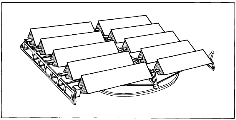
Figure 7-10. Full-tracking mechanisms track along two axes. A turntable allows rotation for east-west tracking while gear devices control motion to follow the north-south progression of the sun.
There are many ways for an array to track the sun. The array can be rotated, or alternatively, the light from the sun can be reflected from mirrors that follow the sun's path through the sky (daily and/or seasonally). Sometimes both are moved. The advantages of moving mirrors instead of arrays are several:
- The mirrors have to be rotated only half as much as do arrays, because reflection doubles the effect of the mirror's movements. (Recall the example of the penlight. the mirror, and the face of a clock: With a mirror straddling the 3 and g, light directed from the 11 o'clock position reflects past the 1 o'clock position. Were the mirror moved to straddle the 10 and 4 positions-a displacement of one hour-the same penlight's beam from 11 o'clock would reflect back past 3 on the clock face-a displacement of two hours [Figure 7-11n.
- Since the mirror and not the array is moving, the array is not subjected to as much structural stress; hence there will be fewer mechanical and electrical failures.
Steering Mechanisms
Whether the mirror or the PV array is turned, some sort of structural device and steering mechanism is needed. Much of the design work for support structures can be directly adapted from conventional civil engineering practices, i.e., for buildings. (Conventional engineering wisdom, however, is not suitable for calculating wind-loading deflections.)
The steering for tracking of the sun about a single plane mostly is by rack and pinion devices rotating about a single axis. For two-axis tracking, there are basically three support options: turntables, pedestals, and racks. Each has its pros and cons.
Turntables can carry the largest (heaviest) arrays, but they are the most costly of the three. Pedestals are reasonable to install, but have very limited capacity. Racks are low cost and easily installed but limit the aperture (view) capability of the array.
All mounts have weight limitations. At some array size, depending on the support, either the solar array or the mirror configuration must be divided into segments and each segment rotated in consort with the other.
Segmenting the array (of cells or mirrors) eliminates the need for gargantuan supports and steering mechanisms, but it expands the problem of ground-area needs. Each segment casts a shadow. This shadow is quite long when a segment is rotated to face a lowlying sun. Space must be provided between panel and/or array segments to avoid the shadow from one segment's blocking off light to part of another array segment. The designer, therefore, must trade off the benefits of separation (optimizing the time during which light can be collected), against its liability (long shadows devouring expanses of land). (An alternative is to increase the number of PV modules within an array field to collect more electricity during a shorter period; but storage capacity must then be increased.)
Figure 7-11. There is benefit to turning a mirror rather than an array to follow the sun. An array would have to rotate through the arc described by the moving sun. The mirror (as shown) needs only turn through half the angle. This can be understood better by looking at the phenomenon in reverse. If the sun were just at the "horizon" (3 o'clock) and the mirror were tilted along the 10-4 axis, the sun's reflection would pass back past the 11 o'clock position. If the sun were at the 1 o'clock position (60o arc advance) the mirror would only have to rotate 30o (to the 9-3 position) for the sun's reflection to pass through the 11 o'clock position. A fixed array at 11 o'clock, looking at the center of the mirror, would have the same view of the sun for the two positions of the mirror and sun.
Tracking Device Controls
When solar concentrators are used to boost the sun's intensity by more than a factor of about 10 (depending on the concentrating unit), the solar array or concentrating device must be made to follow the sun in order for it to be effective. Several methods exist for locking onto the sun. Each has its advantage-such as simplicity or accuracy-and disadvantages.
A time controller is a simple device for facing the array or concentrator into the sun. The sun's position in the sky at any time during any day is known. The solar array can therefore be pointed at the position the sun is supposed to occupy at a particular time. One problem with such a controller is a possible lack of sufficient accuracy for sharply focusing systems, which must be accurate to within a thousandth of a radian. Another is that it cannot compensate for deflections of the solar array, which can be caused by temperature and wind.
A more active system makes use of photocells to locate the sun. Usually at least two such photocells at diagonal ends of the array are used, and the array is driven by a mechanism that works to balance out any difference in the sun's intensity at each photocell. Basic systems grounded on this principle are not without their flaws, and they require special logic (computer) circuitry to reacquire the sun after it comes from behind a cloud. (A photocell system without suitable logic, for example, might seek out the sun but become fixed on a clear area of the sky while the sun is beclouded.)
Another control mechanism for locking an array in the direction of the sun makes use of magnets. If the sun is not focused squarely on the PV cell, it heats up an air-filled tube to one or the other side of the cell. The expanding air causes a magnet to move, and this movement is translated into a reactive movement of the concentrating unit. A disadvantage of the method is that its response is not constant with time, and compensating systems are needed.
OPTIMIZING THE USE OF THE SPECTRUM
Putting more sunlight onto a PV cell is one way of increasing PV power output. But if nothing else is done, much of the sun's light striking a cell is not converted into electric energy: The sun's wavelengths are either too long or too short. If too long, they do not have enough energy to generate charged carriers. If too short, they have more than enough energy, with the excess becoming heat.
Splitting the Spectrum
Cells of different materials, as previously noted in Chapter 3, have different energy band gaps. A reasonable ploy to increase the utility of the sun's light therefore would be to split its spectrum and beam the different portions to cells from different semiconductor materials having band gaps corresponding to the energies of the different portions of the sun's spectrum.
The sun's spectrum divides into components any time it passes from one medium to another. The effect accounts for the rainbow during and/or after a rain. A rainbow occurs when water droplets, suspended in the air, are in a position to intercept and refract the rays of the sun and split the sun's spectrum into many individual wavelengths, or colors. Most lens systems are designed to minimize the spectrum-splitting effect, but there are some optical pieces-such as certain prisms-specifically designed to enhance it.
There are other ways of sectioning off portions of the sun's spectrum (Figure 7-12). All light-transparent pieces have the property of reflecting at least a portion of the light incident on them. The amount reflected differs for different portions of the spectrum. Special devices-dichroic mirrors-have been devised to take advantage of this phenomenon. They reflect one color range of the spectrum considerably more than the complementary part and conversely transmit more of the portion not preferentially reflected.
Figure 7-12. The prism decomposes white light into its component colors (a). A dichroic mirror (b) divides the spectrum into two parts-one transmitted, the other reflected. These devices allow selecting portions of the spectrum to which solar cells are most sensitive, thereby improving their efficiency.
Calculations have shown that, by splitting the sun's light into ten different portions and matching these portions with suitable solar cells, 43% of the light can be converted to electricity. This has not been done, but technologists have worked with combinations of two or three cells.
The most obvious advantage of using two or more different solar cells is to increase electrical conversion. It follows that these higher conversion efficiencies reduce the amount of residual heat that must be dissipated from an array. This simplifies the design of the cooling of arrays and/or permits more concentration of the sunlight using the same amount of cooling.
Converting the Spectrum to a Single Color
There is yet another way of optimizing use of the sun's spectrum by the PV cell. That is to take the received spectrum and convert much of it into a single color whose energy corresponds to the band gap of the solar cell. This can be done with specially prepared fluorescent sheets (Figure 7-13). When light strikes the surface of such a sheet, it energizes the electrons within the sheet. When the electrons return to a lower energy state, they release specific wavelengths of light. The light can only escape from the edges of the sheet. The light can be further concentrated by applying reflectorized coatings to three of the four edges not occupied with PV cells.
Figure 7-13. Diffuse light can be selectively enhanced by using an internally reflecting fluorescent sheet. White light enters and excites a particular frequency of light (chosen for its match with PV cells' light-frequency response). Most of the light generated internally cannot escape because of the optical properties of the sheet. In this way a light on the broad area illuminated by the white light is "tuned" and "focused" onto a narrow edge bordered by PV cells.
BIBLIOGRAPHY
Goetzberger, A.; Heidler, K.; Wittwer, V.; Zastrow, A.; Baun, G.; Sah, E. 1979. "Fluorescent Planar Concentrators- Performance and Experimental Results, Status of the u.S. Department of Energy Photovoltaic Concentrator Development Project." 2nd EC Photovoltaic Solar Energy Conference Proceedings. Berlin; April 23-26, 1979; pp. 515-523.
Meinel, Aden B.; Meinel, Marjorie P. 1977. Applied Solar Energy-An Introduction. Reading MA: AddisonWesley Publishing Co.
Shafer, B.D.; Boes, E.C.; Edenborn, M.W.; Schueler, D.G. 1979. "Status of the u.S. Department of Energy Photovoltaic Concentrator Development Project." 2nd EC Photovoltaic Solar Energy Conference Proceedings. Berlin; April 23-26, 1979; pp. 524-531.
Chapter 8
PV Support Equipment
HIGHLIGHTS
A PV array turns out one kind of electricity (batterylike, direct-current), doing best in a defined operating setting. In the real world, it is often necessary to use alternating current (typical of that provided by electric utilities) to work with electric loads that are not ideal for directly linking to the PV array, and to store electricity for times when the sun is not visible. Special conversion equipment, load controllers, and energy-storage devices are available, thereby making PV more practical to use, either in isolated locations, or in areas where utility electricity can be used as backup to the PV system. Among the equipment are inverters for obtaining alternating current from direct-current electricity, batteries and fuel cells for generating electricity when the PV array is "idle," and synchronizing electronics for reliably integrating the PV system with utility-produced electricity.
Figure 8-1. The concepts of AC and DC electricity can be perceived by relating electron flow in a wire to the behavior of ball bearings rolling along shaped surfaces. In AC electricity, the electrons oscillate back and forth in a wire under the influence of a reversing voltage (force) just as a ball bearing (b), when released at the top of one peak, oscillates between peaks under the force of gravity. In DC electricity, a voltage (force) moves electrons in a single direction along the wire, which is lllustrated by a ball bearing that, set in motion by a force, continues in one direction (a).
PV vs CONVENTIONAL ELECTRICITY
There are two basic forms of electricity: alternating current (AC) and direct current (DC). Alternating current is made up of electrons alternately flowing in one direction and then in the opposite direction under the influence of a cycling force (voltage) that acts a part of a time in one and then the opposite direction. A mechanical system representing alternating flow would be a ball bearing under the influence of a force (gravity) set at the top of a sloped device (Figure 8-1). The ball will oscillate between peaks (assuming no friction). In DC electricity, the electrons flow in a single direction, just as the ball in Figure 8-1 rolls along a flat plane once set in motion.
Figure 8-2. The effect of resistance in an electric circuit is analogous to the effect of friction within a pipe in which water is flowing. The force (voltage) driving electrons is opposed by the resistance in a wire to the flow of electrons, just as the force of gravity potential of a head of water in an elevated tank is resisted by the friction of the pipe to flowing water. By constricting the pipe diameter (such as by partially closing the valve) the flow of water is diminished. Likewise, reducing the diameter of a wire restricts the flow of electrons (current) in a wire (assuming no change in voltage). The flowing water can do work-e.g., by turning a water wheel. Electricity likewise is capable of producing work e.g., in the turning of an electric motor.
DC electricity is generated by such devices as batteries and photovoltaic systems. In a battery, electrons gather at an electrode as the result of a chemical reaction within the battery. In the PV cell, the electrons are generated by light and the ability of the PV cell to move charge carriers to opposite sides of the cell.
The electrons move because there is a driving force a voltage-which is characteristic of the electric source, e.g., an electrochemical cell (battery) or a PV cell.
The flow of direct current is analogous to the flow of water in a pipe descending from an elevated tank. Water traverses the pipe continuously, propelled by the force of pressure (caused by gravity potential) of the water in the tank. Obstructions in the pipe will cause the rate of water flow to drop (Figure 8-2)-just as electrical resistance added to an electric circuit (AC or DC) will cause the flow of current to diminish.
Direct current is a perfectly useful form of electricity for many applications. At an isolated location, there is no need to do anything more than use PV-generated electricity and perhaps store it for times when there is no daylight to activate the cells (Figure 8-3). This is possible so long as the devices being powered can use direct current. But some types of motors and appliances cannot be designed for direct current. For example, it is not possible to design a constant-speed, synchronous, direct-current motor. Also, not all PV installations are isolated; nor is it always practical to design a system whose electric needs can be totally fulfilled by a PV supply. Most PV installations thus have some sort of backup electric service.
A complete electricity-management system using PV as its source for power will contain, in addition to the photovoltaic array, one or more of the following:
- Storage devices
- Power-conditioning equipment, including devices to
- - Limit current and voltage in order to maximize power output
- - Convert direct-current to alternating current
- - Match the converted DC electricity to the utility's AC electrical network
- - Safeguard the utility network and its personnel from possible damage caused by the PV system

Figure 8-3. A PV system with storage and power conditioning. Storage can be as conventional as an automobile battery or as exotic as a superconducting coil. A power conditioner must be matched to electric storage and other electrical loads. If storage is accomplished with a flywheel, a power conditioner (in addition to its possible other functions) must convert electric power to mechanical power. For a good many applications, a power conditioner will at a minimum consist of an inverter with a suitable AC waveform generator to operate electrical loads. Other possible power conditioning equipment include current and voltage limiters and safety switches.
STORING PV'S ELECTRICITY
PV arrays are useful energy producers only when the sun is shining on them and thus are unproductive a good deal of the time. Unless the use of electricity is programmed to match those times that power is flowing from the PV source, some sort of storage medium is needed. This extends the availability of electricity through periods when there is no illumination.

Figure 8-4. Several methods are available for energy storage. The flywheel (a) is receiving considerable attention for PV and other systems, but proved systems are not yet commercially available. Pump-storage concepts (c) have been in vogue for many years and are common among electric utilities seeking inexpensive peak-load reserve. (Air storage systems (b) are a variant of pumped hydrostorage, being most suited to small-scale energy set-aside.) Batteries (d) are possibly the most common method for storing moderate amounts of DC power. The battery illustrated is an advanced concept intended to overcome the short life and inadequate recharge capabilities of present-day designs.
If a utility grid is convenient to the PV system, then it can be used as a low-cost way to store electricity. Excess electricity from the PV system can be suitably made compatible with grid electricity. When more PV electricity is being generated than is being used, the excess can be metered and fed to the grid. When the PV system is not providing enough power, the extra amount needed can be purchased from the utility grid.
A utility grid is not always convenient to the PV system. Still, there are many ways to store electricity, directly and indirectly. (Some are shown in Figure 8-4. Partial characteristics for them are given in Table 8-1.) All those that are commercially available are a good deal less than 100% efficient in returning the power that is put into them. (Presumedly the commercialization of superconducting technology [electric flow without resistance] at some time in the future will result in storage devices that return very nearly all of the energy delivered to them.)
One of the most popular storage methods adopted by electric utilities is to use surplus electricity to turn motors to pump water to a higher elevation. There the water can be stored until its energy (of elevation) is needed. The stored water can then be gravity-fed through turbine-generators. This so-called pumped hydrostorage can be quite efficient (65%). Even more efficient in its ability to store energy, however, is the flywheel (80%), although practical commercial-scale units for use with PV have yet to be demonstrated.
Batteries
A widely used method of storing electricity is electrochemical- i.e., battery storage. However, most commercially available batteries are not especially efficient (perhaps 50% of the energy input can be reclaimed). Neither are they long lasting, having lifetimes of fewer than 6 years. They also are very expensive, occupy considerable floor space, and present safety concerns.
The best among present-day batteries are really modified automobile batteries, which have a high initial cost and a limited service life. Such batteries can be cycled (charged only to half-full and discharged to 20% of full charge) fewer than 2,000 times. A small (5-kW) PV installation may require as many as 350 carsize batteries to carry the system through extended sunless periods (3-5 days).
The battery, however, represents more than mere storage capacity. It can serve as a power conditioner (see section on regulators). By being part of the circuit into which electricity from the PV supply flows, the battery keeps the electrical load more nearly constant, and the PV array can be designed to operate more nearly at its optimum power output. Of course, the battery must be protected from being overcharged by a highly productive array, and a darkened array must be protected from current flowing to it from a charged battery. This is readily done by placing protective electronic components (diodes, which limit the flow of electricity to a single direction) and devices (comparable to automobile voltage regulators) that prevent battery overcharge while maintaining a uniform system voltage. (Note that a battery storage system without a regulator must be larger than one so equipped because it must be large enough to ensure against overcharge.)
Fuel Cells
Fuel cells, per se, are not storage devices. But they can be integrated as part of storage systems for some PV setups. (They, however, would not be suitable for residential PV applications.)
An operating fuel cell is somewhat akin to a working battery. There are two electrodes (one positive, the other negative) in each, and there is an electrolyte separating the electrodes. The difference between the two electricity-producing devices is that a battery stores power within it; a fuel cell can only produce electricity if its electrodes are fed appropriate chemicals. One fuel cell that is relatively well-developed technologically, feeds on hydrogen and oxygen to produce electricity and water (Figure 8-5). (Hydrogen gas introduced at the positive electrode [anode] loses electrons; the hydrogen then crosses over through the electrolyte to the negative electrode [cathode] where it combines with oxygen that has captured extra electrons. The process leaves the anode with a surfeit of electrons; the cathode with an insufficiency. A wire connecting the two electrodes acts as a pathway for the electrons [electric current], which flow in order to correct the electron imbalance.)
It is possible to use a surplus of PV-generated electricity to split water into hydrogen and oxygen (using the process of electrolysis) and then store the hydrogen gas for operation of a fuel cell when reserve electricity is needed. (The oxygen need not be stored since it can be supplanted by air for fuel-cell use.) At the present time, however, fuel cells present some obstacles for anyone contemplating their use in a PV system: Storage systems for chemicals used with today's most practical fuel cells can consume appreciable space or additional energy. Expectations of returning more than 35% of the energy output from a PV array using fuel-cell storage are probably not possible.
Table 8-1. Energy Storage System Key Characteristics: Availability and Applicability
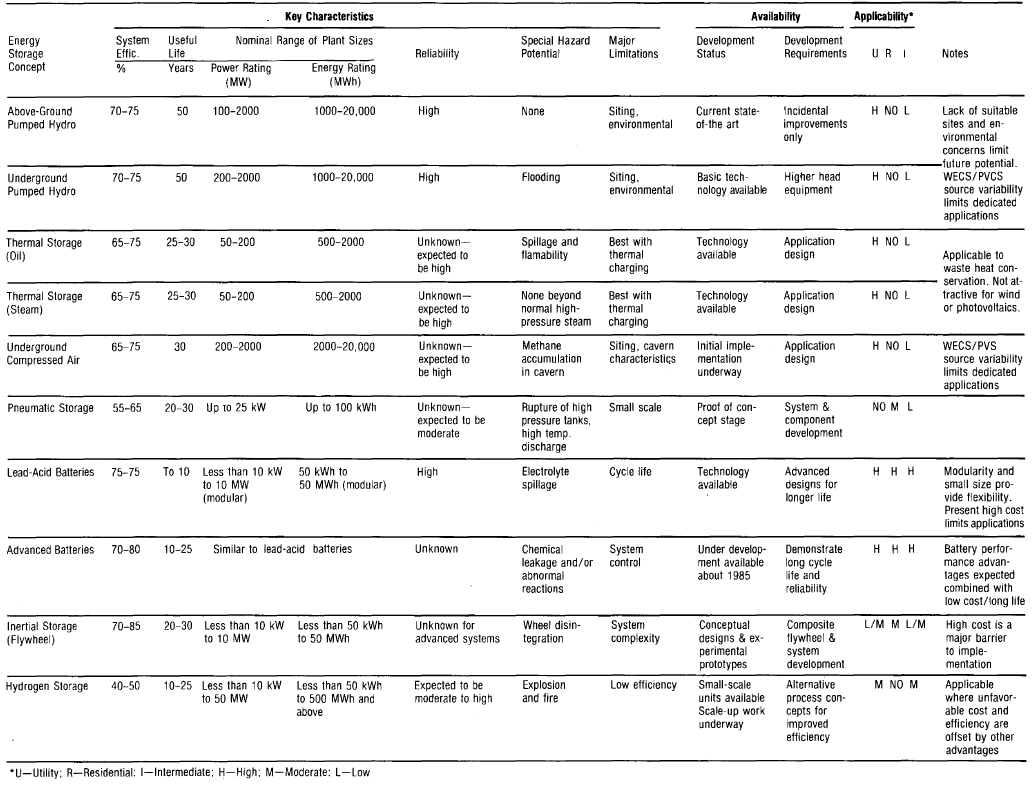
Figure 8-5. Fuel cells have traits similar to batteries. Like batteries they have two electrodes and an electrolyte. However, the fuel cell must be fed ingredients such as oxygen and hydrogen to produce electricity, whereas the battery stores electricity in the electrolyte separating the electrodes.
POWER CONDITIONING EQUIPMENT
In addition to storing electricity, it is often desirable or necessary to process the electricity to make it suitable for the load.
The Inverter
A device, called an inverter, can be installed in the system when it is desirable to convert PV's directcurrent electricity to alternating current. An inverter provides a factor of compatibility, but its use can reduce the array's available electricity if it is not suitably designed to match the electrical load. (Efficiencies as high as 90%, however, are conceivable.) Essentially an inverter is a set of automatic switches that provide polarity reversals from the solar array (Figure 8-6). The simplest DC to AC conversion can be achieved by powering an AC generator with a DC motor. In general, however, electronic switching circuits are used.
If an inverter is to connect with the utility grid, its electricity must be matched to the grid's. The simplest way of matching inverter 'and grid supplies is to use the grid voltage to trigger the switching device.
If there is no utility-grid interconnection, then the direct-current supply need only be converted to an alternating current output that will suitably power the AC equipment on hand. For many electrical devices, the inverter's output need be only a rudimentary, suddenly positive, suddenly negative, square waveform (Figure 8-6). But some equipment (audio systems, and fluorescent fixtures in particular) require an electric signal that smoothly changes between positive and negative alternating-current phases. Some electrical equipment can be operated by alternating current containing lots of add-in frequencies. Other equipment requires AC electricity that is quite free from such impure waveforms. In the latter case, inverters are more costly since they must include filtering systems to remove the spurious frequencies.
Figure 8-6. An inverter essentially is a switching device that regularly flips polarities at the output terminals. A DC motor driving an AC generator is an inverter. In the system illustrated, when switches 1 and 2 are closed the AC output is positive at the left terminal. When switches 3 and 4 are closed the positive AC terminal is on the right. Opening and closing, alternately, the switches in pairs (1/2 and 3/4) produces square waveform as shown in the bottom portion of the illustration.
Regulators
It is often important in the operation of a solar-cell array to control output at some constant level of voltage and current in order to maximize output.
Power Regulators. Where efficiency is a consideration and load control by battery is either insufficient or lacking, power-supply regulators should be a part of the control circuitry. Power regulators for PV systems are devices that sample the current and voltage in the load circuit and then through the use of variable resistance electronic components return the overall resistance of the load to an optimum value to compensate for off-point operation.Some power is consumed in the operation of such control devices; but they can keep overall system operation at a higher level than if they were not present.
It is possible to design some PV systems to avoid power regulation, relying instead solely on regulating voltage.
Voltage Regulators. There are several types of voltage regulators, both mechanical and electronic. Voltage regulators were briefly mentioned previously in covering battery protection from overvoltage. Nominally, a voltage regulator is a variable resistance that absorbs excess voltage. Depending on the design, it can compensate for changes in voltage losses in a load or voltage variability of the supply. One electronic (shunt) type increases the current within the resistance that is a part of the solar array only (and not of the entire system) to compensate for increased voltage drops across the load. Another design decreases the current within the resistance of the solar array to compensate for voltage increases in the photovoltaic system's output.
Voltage Regulators.
Most other power-related equipment placed in a PV system is likely to be present because the PV system is hooked to a utility grid. In such cases, it is important that meters record the quantities of electricity being sold to an being bought from the utility. Other pieces of PV system equipment that utilities probably will require are automatic lock-out switches or isolation transformers. These devices ensure the separation of the PV and utility-grid systems in the event of a grid failure.
SYSTEM ANALYSIS
Choosing the optimum system is not simply that of choosing the best equipment; it is a matter of choosing the equipment that is best for the system. The best system is, in fact, the cost-effective one that most suits electrical needs and whose components are integrated so that overall performance is optimized. Some systems will be as simple as a PV module and a load. Others will include the most highly sophisticated forms of power-enhancing and -conditioning equipment.
The first step in developing a PV system is to assess the application and its environment. To do this involves deciding on the power needs of the loads and the times during which the loads are applied. It also involves establishing the conditions of sunlight (angle, intensity, duration, etc.) and the weather in which the PV system will be operative.
Figure 8-7. The sequence of procedures in designing a PV system. Constraints playa vital role in zeroing in on a PV system design. 'Other Phases' refers to iterations that account for fine adjustments such as shadowing effects.
Design Procedure
The initial design phase of a PV array encompasses choosing the desired power level and load conditions, power-conditioning and load matching approaches, and cell and collector types (Figure 8-7). A series-parallel wiring pattern is selected and matched against the collector/cell types to determine a collector mounting configuration and arrangement.
Next, the package is designed for protection against burnout by properly locating blocking and bypass diodes.
Finally, array performance is optimized by evaluating its response to various illumination conditions and making fine adjustments in the series-parallel arrangement among modules and arrays.
Values calculated at each step bear on those steps preceding, and the design process becomes one of successive approaches to a final design within constraints.
Design Constraints
Design constraints are the key to the system's successful outcome. They provide clear direction and reduce the scope of economic and system analyses and should be continually referenced throughout the design process. Typical design constraints (Figure 8-7) apply to any system and are modified, expanded, and "personalized" for a specific application. Some typical questions inherent in design constraints are:
- Will the system output be AC or DC or both?
- How pure must the electricity be for the load?
- Will the thermal energy generated be used?
- How much of the electric- or thermal-load profile can be economically matched with the available area?
- Is a utility interface available at the location?
- Will there be unavoidable shadow?
- Will the system be actively cooled?
- Will the collectors be flat plate or concentrating?
- Will the collectors be fixed or tracking?
- Does the work proposal specify a type of system or specific design feature?
Other Considerations
The system's analyses* should answer such general issues as the desirability of battery storage, power tracking, concentrating collectors, active cooling, utility interface and various cell technologies.
*The SOLCEL Program available from Sandia Laboratores, Albuquerque. Photovoltaic Systems Definition Project Division, is useful for this kind of work. Concentrating, nonconcentrating, ( tracking, and nontracking systems are available for simulation. Other subsystem models included are power conditioning, energy storage, and either utility or diesel-generator backup.
Data should be collected on cost, availability, and performance of power-conditioning equipment, collectors, PV cells, cooling systems, monitoring equipment and other related equipment that meet design constraints. These data typically include expected lifetime, reliability, maintenance requirements and cost, operating specifications, size, weight, safety features, and many more.
A market survey and generic studies can narrow the candidate hardware combinations that are suitable. These are analyzed to develop details such as collector sizing and orientation, power conditioning and energy storage design, and coolant velocity and temperature.
Based on these analyses, the most promising hardware combination is chosen for analysis of optimum design parameters. Hardware selection or preliminary design options may require updating and reanalysis.
Each PV setup is unique. There is no one fixed or one best design. Certain designs can provide highest-level performance within certain constraints. The designer must be able to trade back and forth among available equipment and the way in which they interact in view of system requirements.
BIBLIOGRAPHY
Silverman, J. 1980. Energy Storage: Oxford, England: Pergamon Press.
Turfler, RM.; Lambarsk, T.J.; Grant, RW. 1979. Design Guidelines for Large Photovoltaic Arrays. SAND 797001. Sandia, NM: Sandia Laboratories for the U.S. Department of Energy. Available from: National Technical Information Service, U.S. Department of Commerce, Springfield, VA 22161.
Chapter 9
PV's Future
The use of solar cells is limited only by the imagination. All the needed technical know-how exists to design photovoltaics for application to any system. There are many areas, even today, where photovoltaics can be practical and/or cost-effective for producing electricity (Table 9-1). However, considerable work remains to develop a broad range of long-lasting, practical, affordable devices. Time will tell whether forecasts of the applications seen for PV (Table 9-2) prove correct.
Photovoltaics has two directions in which to grow: off-grid and the grid-connected applications. The successful penetration of either into the marketplace depends on how effectively a particular application competes with other energy-generating technologies.
Table 9-1. Present Arrays
| Applications | Characteristics |
| Small diverse, custom markets, | Multiplicity of noncompatible designs, Each manufacturer's line adaptable to wide applications and geared to handassembly operations. |
| Projects needing less than 1000 watts of low-voltage (less than 40-volt) DC,generally to charge storage batteries | Modular design suitable for hookup to typical lead-acid batteries. Electrical safety not of concern. |
| Price-insensitive markets capable of sustaining a high price per watt(space and laboratory markets), | Proved-reliability performance |
| Areas subjected to widely varying environmental extremes (remote areas), | Designed for low maintenance under environmental extremes. |
OFF-GRID APPLICATIONS
Off-grid applications possibly offer the biggest potential for PV's uses at the present time because the cost can often be justified compared against alternatives (Figure 9-1). By definition, "off-grid" means not being tied to an electrical network, usually because of the network's not being readily accessible. Certainly spacecraft applictions-at least those restricted to exploring the inner planets-remain high on the list of off-grid PV applications.
In many terrestrial off-grid cases where moderate amounts of power (a few kilowatts peak [kWp] are required, PV's conventional competition is the dieselelectric generator. Even at PV prices prevalent during the early '80s, electricity from PV often cost less than that from diesel power at remote installations.
Table 9-2. Future Arrays
| Applications | Characteristics |
| Large markets, each supporting significantly different array designs and mass production methods | Distinct mass-produced designs for significantly different applications and standardized interchangeability between manufacturers providing for the same application, |
| Loads at high-power, high-voltage AC. | Modular; consistent with industrial, commercial, and residential electrical, codes for insulation, grounding, and safety. |
| Markets with energy costs consistent with electric-utility rates, | Low-cost, long-lifetime designs. |
Markets demanding improved and/or additional functions such as:
| Designs including improved cost! benefit. |
Other off-grid applications appropriate for use with PV are those where equipment is not readily reachable for maintenance. They include power packs for remote communication relay stations, use of an electric-potential generator for countering the electrochemical potential that causes corrosion in metal pipelines, and power for automated weather stations, among others (Table 9-3).
Low-power applications also are likely candidates for PV's use in off-grid situations. They include powering of watches, portable radios, hand calculators, and even small domestic electric systems. These off-grid uses are expected to grow, eventually to include such applications as outdoor lighting and the powering of moderately sized villages.
GRID-CONNECTED APPLICATIONS
Although off-grid and, in particular, remote off-grid applications have a significant place in the growth of a PV industry, PV technology is not expected to flourish until it can successfully compete in the utilitysupplied, grid-connected market. This market has two facets: distributed and central station electric sources. The former consists of PV installations buying power from and selling power to the utility, while the latter are the utilities. Acceptance of PV for central-station application will depend on many factors including cost (foremost) and reliability.
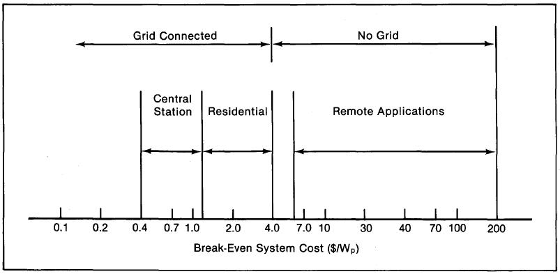
Figure 9-1. Cost-justification chart for PV systems (i.e., with equipment). Many off-grid applications using PV could be justified during the 1980s as preferable to those with other power sources. Although perhaps initially more expensive, minimal maintenance makes PV a superior choice for isolated-area use. Costs for residential use were severalfold higher than justifiable for general acceptance during the early '80s. (PV systems' costs are about a factor of 1.5 or greater than array costs.)
Central Station Production
Utilities conceivably have the option of using PV generated electricity in two ways: for base load or for peaking load. Base-load application at large utilities will require the greatest progress in PV systems development because it can only be feasible where directly competitive with turbine-generated electric power (derived from fossil and/or nuclear fuels). Experts within the Federal Government plan that the cost of PV modules will be reduced to less than 50¢ per peak watt (in 1980 dollars) by the year 2000, enabling PV's use for base-load applications.
Some other experts are of the opinion that PV costs will be brought down to approximately $1 per peak watt (1980 dollars) by the turn of the century. However, even at this level, broad possibilities exist for PV application by utilities. Primarily, PV systems will be able to compete directly almost everywhere with diesel-engine-generated electricity.
A number of experts on PV economics believe that PV's being competitive with diesel-produced electricity will make PV systems suitable for low-to-medium- power electricity generation at utilities dependent on diesel generation. Some experts also contend that PV systems that break under the $1 per peak watt level will enable PV to compete at utilities for providing peak-load generation-at least in areas where. peak loads do not extend into non-daylight hours.
Distributed Production
Other experts contend that another, possibly better, solution to peak loading is the distributed production of PV-that is, homes and businesses with individual PV systems feeding into the utility's grid.
Inroads by PV into the distributed production of gridapplied electricity depend on PV's acceptance for such application by utilities and potential users of the concept.
There is some skepticism about individual tie-ins to grids. Tie-ins could lessen capital needed by a utility for base-load or even peak-load generating equipment, but many utility managements are still looking at the issue. Possible disturbances to grid systems are also eyed with concern, as are potential safety problems.
Table 9-3. Examples of Present Terrestrial Applications of Photovoltaic Power Units
| Application | Peak Rating (W) |
| Warning lights: | |
| airport light beacon | 39 |
| marine light beacon | 90 |
| railroad signals | |
| highway barrier flashers | 1.2 |
| tall structure beacon | |
| lighthouse | |
| Communications systems: | |
| remote repeater stations for | |
| -microwaves | 50 |
| -radio | 109 |
| -TV | 78 |
| remote communications stations | 3500 |
| portable radio | 2400 |
| emergency locator transmitter | 50 |
| Water systems: | |
| pumps in desert regions | 400 |
| water purification | 10800 |
| Scientific instrumentation | |
| telemetry-collection and transmission platforms for environmental, geological, hydrological, and seismic data | |
| anemometer | 100 |
| Remote pollution detectors-H2S-noise | 3 |
| Industrial: | |
| remote machinery and processes, e.g., copper electrolysis installation | 1500 |
| cathodic protection of underground pipeline | 30 |
| electric fence charger | |
| domestic water meter | 20 |
| off-shore drilling platformsb forest fire lookout posts | |
| Battery charging: | |
| boats, mobile homes and campers, golf carts construction site equipment | 20 |
| NI-Cd-powered military equipment | 74 |
| Recreational and educational: | |
| educational TV | 35 |
| vacation home | |
| -lighting, TV | |
| -refrigerators | 200 |
| sailboats | |
| -lighting, ship-shore communication | |
| -automatic pilot | 66 |
| portable TV camera camping lighting electronic watches, calculators | |
| recreational center sanitary facility | 168 |
| Security systems: | |
| closed circuit TV surveillance | 150 |
| intrusion alarms | 6 |
Government's role enforcing laws to bring about utility acceptance may largely determine PV's growth in the distributed grid-connected market.
The cost factor also will be most decisive in the growth of distributed, grid-connected PV. If utilities buy back electricity from producers at reasonable prices (greater than half the utility's selling price) and the cost of the distributed installations can be reduced to less than 75¢ per peak watt (with subsidies if necessary), many analysts believe that broad acceptance of PV-grid applications will be achieved.
Acceptance Problems
Other factors must be considered for PV to gain wide acceptance by the year 2000. They include:
- Lack of user awareness
- Time lags in user acceptance (all markets)
- Lack of PV and building-code standards and certification
- Investment in and commitment to existing powersupply systems
- Lack of available and dependable maintenance services
- Lack of suitable financing and insurance (grid markets) programs
- Public resistance to utility ownership (grid markets)
- Uncertainty about buy-back utility rate structures
- Legal barriers. including uncertainty regarding solar access and utility acceptance of home systems
- An information void
- Substantiation of suitable system lifetimes
- Lack of suitable optimal design criteria
- Lack of standardization criteria
AIMS
Some of the PV technical difficulties that remain may be overcome by a graduated process, which appears to be underway as the result of Japanese approaches. Using amorphous silicon Japanese plans seem to call for using PV for a great number of small low-powered applications, including radios, wristwatches, and hand-held calculators. They intend to increase PV-cell production capacity and simultaneously improve PVcell efficiency as demand for these electronic products grows. The improved PV technology will be progressively transferred to larger applications, easing acceptance problems. Using this approach, Sanyo, for example, expects the public and the engineering community to be receptive to, and PV cell manufacturers prepared for, a PV power-production industry that will produce electricity for less than 10¢/kW-hr using cells costing 15¢/Wp by 1990.
The United States Government and private-sector actions have been directed at eliminating acceptance problems. During the mid 70s, the Federal Government began taking an active interest in rapidly developing PV. At that time, government sources concluded that $1.5 billion would be needed each year to finance research to achieve 1980 goals (Figure 9-2). Research was begun to gather the data needed to determine the design factors for use with standard-type installations and to develop information relative to the reliability of the proposed designs in different areas of the country. Government-funded programs were created to develop these and other data, including those for costreduction methods and materials. Among the goals of the federal 1978 Solar Photovoltaics Energy RD & D Act were: (1) increases in the amount of electricity produced by PV from an insignificant fraction of the total U.S. output to about 4 giga watts (GW) peak by 1988, and (2) something in the vicinity of 20 GW (or 1%) of U.S. needs by the year 2000.
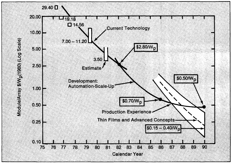
Figure 9-2. Department of Energy costltimeline chart, conceived in the late '70s. As of the early '80s prognosis was running about three years behind schedule.
The federal photovoltaics' program has several major thrusts. By far the largest is aimed at substantially reducing crystalline silicon array costs and greatly increasing production capability. Government's involvement had been primarily for engineering development and market stimulation, including a series of scheduled array purchases, which, although small by electric-utility standards, are sizable for the PV industry. The government has sponsored several research projects in its efforts to develop PV technology for commercial use. The goal is to get the kinds of data that only in-use projects-located at different areas of the country and supplying different kinds of loads-can provide. Among the test facilities for residence application are the Carlisle House in Massachusetts and the John Long home in Phoenix, Arizona (Table 9-4). Several "commercial" application test sites, such as that for the Air Force at Mt. Laguna, California, also have been funded. Some industrial-sized installations (less than 200 kW) have been funded by DOE (mostly in the sunbelt) to serve as possible prototypes for large central stations. They include a flat-plate installation being operated by Lee County electric utility in Lovington, New Mexico, and a concentrating collector design for Arizona Public Service.
For their part, utilities (individually or through representative associations) intend to stay atop the state of the art and ensure that utility-industry requirements are available to the federal photovoltaics program. Utility photovoltaic activities will complement federal efforts, with electric-utility requirements and impacts as a prime focus. Toward this end, the Sacramento Municipal Utility District has given serious consideration to designing an operable utility-sized plant (100 MW, to be built in stages, starting with 1 MW), but the project hinges on receipt of federal funds.
Table 9-4. Laboratory PV Houses
| Project and Location | Operational Date | Peak kW Power* | Array Area (ft2) | Array Cost 1000$ |
| Carlisle House, Massachusetts | March 1981 | 7.3 | 1000 | 131 |
| Cape Canaveral, Florida | Aug. 1980 | 5 | 55 | |
| Arlington House, Texas | Nov. 1978 | 6,2 | 150 | |
| Hawaii- | ||||
| 2 retrofits | 1.9,3.8 | |||
| 1 new home | Feb. 1981 | 3.8 | ||
| John Long House, | ||||
| Phoenix, Arizona | May 1980 | 6 | 120 | |
*To convert peak kW to annual kWh supplied by the array, multiply peak kW by 1500 (a very approximate rule-of-thumb).
Efforts by the Electric Power Research Institute (EPRI), which represents many U.S. utilities, will determine nominal cost and performance objectives for central photovoltaic power plants, which when combined with several hours of storage, can serve medium loads. The objective would be for such plants to displace oil- and gas-fueled generation plants for adding extra capacity to base-load generation while giving the high overall grid reliability required by electric-utility systems. Objectives will be reviewed as changes occur in photovoltaic and conventional generation technologies and economics.
An additional key element in EPRI's investigation of PV is a utility-oriented requirements assessment within different geographical regions. This is being done to come up with the best designs, varying the combination of available components for utilities of different sizes, customer mixes, and locations.
Also the potential environmental impacts of photo) voltaic central power plants are being studied as part of an environmental assessment of major solar central station alternatives.
This document has been designed to emphasize crystalline silicon because of its relative simplicity and illustrative value. However, much of the breakthrough research in PV is going on in other materials-especially thin films (less than 10 micrometer thickness) like amorphous silicon, indium phosphide, copper indium selenide, and gallium arsenide. The advantages of thin films are that they are less expensive to make into cells while it may be possible to attain reasonable (10%) efficiencies. The future progress of PV will involve materials other than single-crystal silicon.
PV has a definite role to play in the U.S. energy future. How much and how fast will depend on private industry's and government's commitment to develop it.
BIBLIOGRAPHY
Durand, H.L. 1979 (Sept.). "Present Status and Prospects of Photovoltaic Energy Conversion." Proceedings of the Photovoltaic Solar Energy Conversion Conference (C21). pp. 93-105.
Ehrenreich, Henry; Martin, John H. 1979 (Sept.). "Solar Photovoltaic Energy." Physics Today. Vol. 32 (No.9); pp. 25-32.
Balzhiser, Richard E. 1977 (June/July). R&D Status Report. "Fossil Fuel and Advanced System Division." EPRI Journal.Vol. 2 (No.5): pp. 49-51.
Magid, L.M. 1979. "The U.S. Department of Energy National Photovoltaics Program Plan." Proceedings 2nd E.G. Photovoltaic Solar Energy Conference. April 23-26. 1979. Boston, MA: D. Reidel Publishing Co.; pp.1113-1126.
Ross, KG., Jr. 1976. "Interface Design Considerations for Terrestrial Solar Cell Modules." Proceedings 12th IEEE Photovoltaic Specialists Conference - 1976. New York, NY: Institute of Electrical and Electronic Engineers, Inc.; pp. 801-802.
Stiller, P.H.; Eichler, C.H.; and Kilar, L.A. "Interconnection of On-Site Generation with the Electric Utility -Site Owner Concerns." Proceedings 14th IEEE Photovoltaic Specialists Conference-1980. New York, NY: Institute of Electrical and Electronic Engineers, Inc.; pp. 240-245.
